One of the main messages from the forum is that embedding passives into package substrates is just beginning for applications ranging from consumer electronics to routers. Embedded active in substrate has seen few commercial implementations but it is thought will grow in importance with time.
JISSO has defined "embedded substrate" as containing embedded active or passive components or passive functions that are fabricated as part of the substrate fabrication process.
 1
1Jan Vardaman of TechSearch presented an overview of the embedded substrate market. Advantages of embedded components are:
- Small form factor (reduced Z-height), enables reduced board thickness
- Improved performance
- Shorter electrical path, EMI reduction, integrated passives
- Shielding advantages for RF components
- Embedded die technologies appropriate for:
- Lower value, high yielding die where high interconnect density is required on both sides of the substrate
- RF modules where embedding tested die allows high density SMT on top
There are still concerns about:
- Patent issues
- Handling thin die
- Solder joint reliability of buried joints
- Cost (embedded die cost vs. die in package mounted on board)
- Concerns about liability
- Test (how to test after embedding component?)
- Inspection (how to inspect an embedded component?)
Takayoshi Katahira of Nokia addressed embedded technology from the mobile device perspective.
Embedding technology can either be face up:
- Cavity cut-out
- Component placement
- Lamination
- Laser drilling
- Plating
Or it can be face down, where the component is soldered in place and then buried. E-B2IT is seen as the leading technology of this kind.
Since 3D eWLB and RCP fan out technologies enable the same merits as substrate-based embedding, these can also be called "active embedding." Nokia sees high IO active embedding into packaging substrate coming soon.
Top-Bottom interconnection and top patterning enabling 3D assembly will be suitable for:
- Standard memories with high-pin count
- DDR2 Quad Channel or DDR3
- WLCSPs
- Passives

Many passives are mounted on mainboard for smartphones. Capacitors tends to be used in the greatest numbers. Soldering embedded caps has a clear advantage in process cost.
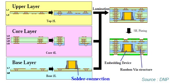
Bruce Su of ASE presented chip embedding as a technology evolution after bumping. ASE is developing "advanced Embedded Assembly Solution Integration" or aEASI as shown below:

EASI currently has the following design rules:

For all the latest on 3D IC integration and advanced packaging stay linked to IFTLE..........
No comments:
Post a Comment