Monday, August 19, 2013

IFTLE 159 Semicon Suss Wkshp part 1: Material Suppliers; IEEE 3DIC Program

Am I the only one who missed Semicon West ?


I had a full week of workshops and 1-on-1 meetings set up for Semicon West, but … Due to the Korean crash, United canceled my Sunday flight and rebooks me for Tuesday night (I’m a million mile flier so imagine the service the peons got !) then my replacement Delta flight was cancelled on Monday again with no seats on flights into SF, Oakland or San Jose till late Tuesday. I finally concluded some things are simply not meant to be.

The Suss technology forum that I helped set up and was set to moderate went on without me so I’d still like to cover some of the materials that were presented there.

Lets look first at the material suppliers.

Lord

Le of Lord gave a presentation on their photo definable silica filled epoxy “solder brace” material which they propose to use as a final passivation in a standard WLP redistribution process.

We are shown data concluding that the “solder brace” shows better thermal cycling reliability (-40 to +125 C) and drop test results then an unidentified “PI” , but without clear understanding the identity of the PI and all the design dimensions involved (such as thickness of the screen printed epoxy vs the spun PI) it is hard to draw any substantial conclusions from the data.

Since screen printing is not a usual unit operation in a standard redistribution process this might be a barrier to acceptance for such a filled product.
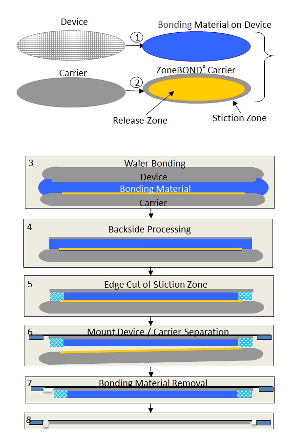
 
Brewer Science
Smith of Brewer Science detailed the separation technologies available for their ZoneBond Process. The temporary adhesive ring of the ZoneBond process can be removed either by immersing the temp bonded wafer on a perforated carrier in a solvent bath as shown below:


Or,  by trimming the narrow bonded ring post fabrication to release the device wafer, where:
-          Debonding occurs at room temperature.
-          Separation occurs at the carrier-to-adhesive interface, not the adhesive-to-device interface.
-          Device is mounted in the film frame and is firmly supported on a vacuum chuck during debonding.
 This allows higher-temperature-capable adhesives
-          Thermally stable in bonded pair to 240°-260°C (depends on processing parameters)


Dow Corning
Ho of Dow Corning presented their new silicone based bi-layer temporary bonding solution. Their Bond/Debond Process Flow is shown below.
- Spin-coat bi-layer (release and adhesive layer)
- Room temperature bonding / debonding
- post-bonding cure on hot plate
- no plasma or lasers necessary
- fast mechanical debonding


Dow Chemical
Gallagher of Dow Chemical detailed their photo and laser patternable plating resists and dielectrics for WLP and 3D TSV.
Their Novolac (positive) and Acrylate (negative) resists are capable of a brad thickness range.


Their Cyclotene (BCB) dielectrics are laser patternable and their Intervia (epoxy) dielectrics show excellent vertical sidewalls. They also highlighted BCB as a temporary bonding solution which shows high thermal stability during backside processing ( , 1% weight loss at 300 C per hr) and clean RT mechanical peel-off debonding.   
Suss
Lutter, of Suss, compared the temporary bonding solutions that Suss supports focusing on the room temp mechanical debonding solutions.
 
 
The mechanical release at RT is described as follows:


Zonebond and several other solutions show excellent TTV (2-3um) after thinning to 50um.


Flex frame tape is a key to good debonding and cleaning . The principle of Suss debonding is shown below.


IEEE 3DIC
The IEEE’s premier 3DIC conference is on tap for the USA again this year. The conference will be held in San Francisco the first week of October. You can register here [link]
Lets take a look at the program:


 Wednesday, October 2nd  - Free Tutorials !
 13.00 – 14.00 Tutorials: 2.5/3DIC Players, Products & Markets, Rozalia Beica – Yole Developpement
14.00 – 15.00 Tutorials: 3DIC - Prof. Mitsu Koyanagi, Tohoku University
15.00 – 16.00 Tutorials: Design for 3DIC, Prof. Paul Franzon - NCSU
16.00 – 17.00 Tutorials: TSV and Interposer Design for High Performance and Low Noise,  Kim - Kaist
17.00 – 18.00 Tutorials: Monolithic 3DIC, Zvi Orbach
Thursday, October 3rd
08.30 – 09.45: Keynote Speaker: Prof. M. Taklo, SINTEF, Title:” E Brains”
09.45 – 10.15: Invited Talk I “ 3DIC Activity at Tohoku “  Prof. Mitsu Koyanagi, Tohoku University
13.00 – 13.30: Invited Talk II – “A Perspective on Manufacturing 2.5/3D”  Robert Patti, Tezzaron
17.00 – 18.00: Panel Session “Progress and Outlook for 3D ICs and 2.5D Systems -
Moderator: Jan Vardaman, TechSearch
Friday, October 4th
08.30 – 09.00: Invited talk III “The DARPA ICECool Program”  Avi BarCohen, DARPA
Hope to see you all there ….
For all the latest in 3DIC and advanced packaging stay linked to IFTLE…....


Saturday, August 10, 2013

IFTLE 158 2013 ConFab part 2: Amkor and Siliconware


Finishing our look at the June 2013 ConFab packaging activities.

Amkor
Bob Lanzone, Sr VP of Engineering Solutions for Amkor, like the other OSATS sees smartphones and tablets driving the market moving forward.

 
If you ever wondered who the key players were in each of the mobile phone IC functions, Lanzone used this enlightening slide from  Gartner.


Amkor's update on Copper Pillar technology indicates an expected doubling in demand this year and continued expansion into “all flip chip products”.  

 
Their “TSV status” takes credit for being the first into production with TSMC and Xilinx.

 
Looking at the 2.5D TSV & Interposer Supply Chain they see:
• High End Products : Networking, Servers
- Silicon interposers ; < 2um L/S, < 15nsec latency, > 25k μbumps per die
           - Amkor is engaged with Foundries to deliver silicon interposers today
• Mid Range Products : Gaming, Graphics, HDTV, Adv. Tablets
 - Silicon or Glass interposers ; < 3um L/S, < 25nsec latency, ~10k μbumps/die
             - Not actively pursuing glass interposers yet as infrastructure still immature
• Lower Cost Products : Lower End Tablets, Smart Phones
 -  Silicon, Glass or Laminate interposer ; < 8um L/S, low resistance, ~2k μbumps
              - Must provide cost reduction path to enable this sector
              - Working with laminate supply chain to enable
They are targeting 2014 for their “possum” stacking as shown below:


Siliconware (SPIL)
In the presentation “The expanding Role of OSATS in the Era of System Integration”, Mike MA , VP of R&D for SPIL looked at the obstacles to 2.5/3D implementation and came up with the conclusion that cost is still a significant deterrent to all segments.

 
He discusses the two current business models for 2.5D which are the “foundry model” supported by TSMC and the “collaboration model “ supported by GF and UMC. He now adds a third model “the OSAT turnkey model which is now supported by TSMC.
SPIL is the first OSAT to propose this OSAT centric model where the interposer is fabricated by the OSAT who then assembles and tests modules made with chips from multiple sources.  The impediment to this route in the past has been the lack of OSAT capability to fabricate the fine pitch interposers which require dual damascene processing capability, which until now was only available in the foundries. SPIL has now  announced the equipment for fine pitch interposer capability (>2 layers, 0.4-3um metal line width and 0.5um TSV ) has been purchased and is in place.
Ma indicates that while the foundries are not happy with this SPIL proposal, their customers, especially their fabless customers have been very supportive.  He feels the inherent lower cost structure of  OSATS will have a positive impact on the 2.5/3D market which has been somewhat stagnant since the FPGA and memory product announcements in 2010.

 
SPIL also announced a wafer level fan out (WLFO) program on 370 x 470mm organic based panels which they feel is a potential low cost solution for those with lower density interposer requirements.
 
For all the latest in 3DIC and advanced packaging stay linked to IFTLE…………………..


Monday, August 5, 2013

IFTLE 157 ECTC part 3: SPIL Backside Reveal, Sematech & IMEC Protrusion,SUNY Binghamton on Cu-Cu Bonding


Continuing with our look at the 2013 ECTC.

Siliconware detailed the “Integration Challenges of TSV Backside Via Reveal Processing”.

After via formation, finished CMOS wafers or interposers are temporarily bonded to glass carriers. The TSV are ‘ revealed ‘ by Si back grinding and plasma etch steps, passivated with PECVD nitride, and CMP’ed to open the Cu pillar area. The via reveal processes must maintain acceptably low

TTV to allow subsequent bonding/stacking steps. Also the process temperature must be lower than the carrier bonding adhesives which is a particular challenge for the dielectric deposition step. The SPIL backside reveal process is shown below.


A major challenge of the via-reveal process is control the exposed copper TSV height, because incoming wafers to via reveal can have significant compounded variation, such as TSV depth uniformity, glass thickness uniformity, adhesive thickness uniformity and Silicon thickness uniformity after grind.

 SEMATECH and RPI reported on their studies on “Backside TSV protrusion induced by thermal shock and Thermal Cycling”

The TSVs used for this study were fabricated on 300mm wafers with a TSV height of ~50μm
and an aspect ratio of ~10:1. The front side of the TSV wafer is bonded face down on a handle wafer and  backside-thinned to reveal the TSV and metallized to form testing lines and pads. The cross section schematic below shows the structure.

 
Various combinations of thermal loads (RT -  200 C - 400 C) and ramp-up/cool-down rates (0.167 C/s to 25 C/s) are used for thermal shock and thermal cycling tests. No TSV protrusion is visible at 200 C or below, while larger TSV protrusions are observed at higher peak temperatures.The avg TSV protrusion height, collected from 108 single TSVs under 3 testing pads over each die, increases from 0.1μm at 250 C to about 0.5μm at 400 C.


The TSV protrusion varies significantly from TSV to TSV, resulting in big error bars. This is reportedly due to the grain boundaries in each TSV (particularly near the Cu testing pads) being very different from TSV to TSV, indicating that the key mechanism for the protrusion could be related to the Cu grain boundary diffusion.
SEM images of the TSVs reveal delamination is observed at the interface between the Cu TSV and the Cu testing pad on top of the TSV-1, while delamination between Cu TSV sidewall and oxide liner is found in TSV-2.


IMEC also reported on protrusion issues in their paper “Impact of Post Plating Anneal and TSV Dimensions on Cu Pumping”
When Cu-filled TSVs are exposed to high temperatures during BEOL processing, compressive stresses arise in the Cu TSV due to the large difference in coefficient of thermal expansion with the surrounding Si. These stresses  are partly relaxed by irreversible extrusion of the Cu, a phenomenon known as ‘Cu pumping’, which may damage  the BEOL layers on top of the TSV. In order to reduce the amount of Cu pumping during BEOL processing, a high temperature anneal step can be applied after TSV plating and before Cu CMP.
IMEC, who is generally given credit for offering an anneal solution  protrusion problem in 2011 has now  used optical profilometry to study residual Cu pumping in TSVs with different post-plating anneals and different TSV dimensions ( 5 x 50um vs 10 x 100um ). In total ~ 4000 TSVs were inspected. Within one sample the Cu pumping values show  an intrinsic large spread, therefore the distribution tail rather than the median is determining the impact on BEOL reliability. Lower pumping was found in TSVs annealed at higher temperatures and for longer times. The sinter conditions of 20 min at 420 °C were confirmed as optimal post-plating anneal conditions.. However, in order to effectively control the impact on BEOL reliability, development efforts should also be aimed at reducing the Cu pumping distribution width.


SUNY Binghamton and SEMATECH presented their work on the “Mechanism of Low Temp Cu-Cu Direct Bonding for 3D TSV Package Interconnect”.

While the solder-based approach for connecting chips to packages or chips to chips has become the industry standard for at least the first generation of 2.5/3D products, but the potential to significantly drive this approach to finer pitch interconnects is limited. The leading method for fine pitch chip-to-chip interconnects (pitch of 10 microns or less) is generally believed to be Cu-Cu direct bonding. In the direct bonding of Cu to Cu, the flatness of the surface on a small scale (~1 micron) or a large scale (wafer or die scale) and the chemical condition of the surface play important roles in the quality of the bond. Other factors such as the Cu grain size and grain orientation may also impact the quality of the Cu-Cu bond.
 Therefore, it is necessary to use a reducing gas to decompose the oxides. Forming gas, which is a mixture of H2 and N2, can provide such a reducing environment to decompose copper oxides effectively.  Prior attempts to surface passivate / clean including self-assembled monolayer passivation , plasma cleaning and chemical mechanical polishing with a formic acid clean all result in  improved bond quality as a result of the passivation and cleaning approaches used. The Bingham / Sematech group CMP’ed the copper in the presence of benztriazole which protects the copper surface during CMP, but does not prevent oxidation once the CMP is complete. The cleaned surfaces were then exposed t atmospheric conditions for varying times and reexamined by XPS (Xray photoelectron spectroscopy)
 Cu2O and CuO can observed on the clean Cu surface after a short atmosphere exposure (1 minute), while Cu(OH)2 and/or CuCO3 can be observed on the surface after longer exposures longer exposures (>30 minutes).
 Wafers were cleaned by Ar sputter cleaned (NA) or annealed at 200ºC in forming gas (FGA).  Both wafer pairs were bonded within minutes after cleaning by thermo-compression bonding with a force of 80 kN at 195°C for 5 minutes. Samples of NA and FGA wafers exposed to the atmosphere for 30 min and then examined by XPS showed both CuO and Cu2O but no Cu(OH)2 .
The  NA and FGA Bonded Wafers were characterized by CSAM looking for voiding. The image of the bond interface for the FGA wafers indicates  an absence of voids for almost the entire interface, whereas the image of the bond interface for the NA indicates voids throughout the interface. They attribute the better bonding for the FGA wafers to more effective Cu oxide removal by the forming gas anneal.
 For all the latest in 3DIC and advanced packaging stay linked to IFTLE……………………….


C.