Saturday, July 7, 2012

IFTLE 109 2012 IEEE VLSI Conference ; Lester’s cousin CFL Dies Prematurely


The  IEEE Symposium on VLSI Technology  is sponsored by the Electron Devices Society -- ED and the  Solid-State Circuits Society -- SSC. At this year's conference, Micron gave further details on their hybrid memory Cube and TI detailed their studies on TSV induced stress on 28nm CMOS and Chuo Univ described a hybrid NAND + ReRAM SSD stack with better power consumption and product lifetime.
Hybrid SSD memory stack with ReRAM and TSV

Perofessor Takeuchi of Chuo Univ described a hybrid SSD architecture using ReRAM and high capacity NAND flash memory.

When SSDs are used for servers in financial institutions, performance is hindered and power consumption increased because random access is dominant. This causes data to get split up if the size of the data packets are not of the appropriate size (minimum for NAND is 16Kb). Takeuchi's memory stack combines a NAND flash memory and ReRAM. ReRAM is used as both cache and storage memories. To overwrite a small amount of data in the NAND flash memory, software transfers the page of data to the ReRAM so that data is not fragmented in the NAND flash memory.

(Click on any of the images below to enlarge.)


A prototype, tested on an emulator, showed that compared with existing SSDs which only use NAND, the hybrid memory stack achieves an 11X higher data writing performance, 93% lower power consumption and 6.9 times longer product life. This assumed that the controller, ReRAM and NAND flash memory were connected by TSV. Although this has been hyped up by several reporters, we should note that it is possible to achieve almost the same results without using TSV. The major gain of using the TSV appears to be a 14% decrease in energy required to write as shown in the comparative table below.  


It is proposed that SSD in data centers would have to be changed out about 7 times less thus reducing expenses.

It should be noted that in order to use  the hybrid SSD architecture for different applications, it is necessary to change the controlling software algorithms.

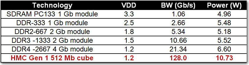
Micron Hybrid Memory Cube (HMC)
We have previously discussed the fact that  Micron has created an industry group to collaborate on the implementation of an open interface specification for a new memory technology called the Hybrid Memory Cube (HMC). [http://www.hybridmemorycube.org/]

The HMC is a stack of multiple thinned memory die sitting atop a logic chip bonded together using TSV. This greatly increases available DRAM bandwidth by leveraging the large number of I/O pins available through TSVs. The HMC requires about 10% of the volume of a DDR3 memory module. It is claimed that the technology provides 15X the performance of a DDR3 module, uses 70% less energy per bit than DDR3 and uses 90% less space than today's RDIMMs. [see IFTLE 95 "3DIC - Time Flies When You're Having Fun; Further Details on theMicron HMC..."; IFTLE 74 "The Micron Memory Cube consortium"]

The HMC device uses TSV technology and fine pitch copper pillar interconnect.  The DRAM logic, responsible for DRAM sequencing, refresh, data routing and error correction is placed in a  separate high performance logic die.  DRAM and logic are connected by thousands of TSV. The DRAM is a slave to the logic layer timing control.  The HMC was constructed with 1866 TSVs on a roughly 60um pitch. 


HMC electrical performance is are compared to other DRAM modules below.


TI Studies Impact of TSV Stress on Electrical Performance

They found that the impact of TSVs on surrounding Si is tensile but that a tensile etch stop layer (ESL) counters the impact of the TSVs on near-surface Si where devices are present. Also, insertion of compressive shallow trench isolation (STI) between the TSV and device will also act to buffer this impact.
They conclude that "...the electrical properties of N/PFETs between 4 and 16um of TSVs are negligibly impacted (less than 2.3%)..." and that For Wide-IO Memory-Logic interface applications employing a 40 x 50 um JEDEC TSV array, ESD and decoupling capacitors which do not contain N/PFETs can be placed immediately adjacent to TSVs such that CMOS logic circuitry does not require placement less than 4 um.
CFL Fails While Incandescent Lester Still Going Strong

When last we discussed our hero Lester the incandescent lightbulb [ see  IFTLE 98 "Lester the Lightbulb vs CFL and LED: the Saga Continues"] we found out that an actual calculation of the cost of various electrical functions in my household revealed that lighting was responsible for $4.31 per month (that’s for operating 30 bulbs) on your electric bill and that saving three-quarters of that by using Lester's lighting cousins CFL or LED would therefore save you about $36/year (if you replaced all 30 bulbs), which is not enough to buy you 1 LED bulb. The CFLs whose price was now down to about $4 each (vs $0.25 for Lester)  promised 9.1 years of lifetime (at 3 hrs use per day). Our test bulbs (CFL and LED) were installed on 08/15/2011 [ see IFTLE 63 "Bidding Adieu to Lester Lightbulb"]. So...cousin CFL lasted less than 11 months (vs the promised 9.1 years). I guess you’d have to call this an "outlier"?
So cousin CFL operated 11 months saving me 1/30 of $4.31 or 14 cents / month or $ 1.54 in 11 months …but remember the bulb cost me $3.97 . You can do the math. And remember since the CFL’s contain mercury, I’m now supposed to contact the EPA for proper disposal instructions (yeah right !) 
Cousin CFL and cousin LED promised me "hope and change"...  "to transform US power consumption as we know it today." So far, I'm down $2.43 and need to replace the bulb. Typical Govt BS !
I guess we can understand now why the Govt. got involved to ban poor Lester from the shores of the US. Would anyone actually buy these CFL or LED bulbs, unless they were forced to ?
Cousin LED is still burning bright as are all the incandescants that were started at the same time. Be assured we will keep you up to date on cousin LEDs health !
For all the latest on 3DIC and advanced packaging stay linked to IFTLE.............................

TI researchers have used NanoBeam Diffraction (NBD) to measure near-TSV Si strain in fully processed wafers. The electrical behavior of poly-SiON P/NFET transistors were characterized for full thickness wafers varying temperature, orientations and proximities to isolated and arrayed TSVs.
NanoBeam Diffraction measurements of Si strain within 5 um of TSVs were acquired for samples prepared from fully processed wafers, showing that for proximity greater than 1.5 um the impact of TSVs is negligible.

Sunday, July 1, 2012

IFTLE 108 2012 ECTC 2: NCF, WUF, MUF for tight pitch Assembly


For those of you paying attention, you will have noticed that IFTLE has been stuck on 107 for nearly a month.

Has all progress stopped in 3DIC ?.....NO

Has all progress stopped in Advanced packaging ?......NO

Are there no new industry rumors  ?......NO

So whats up IFTLE where is our new information ???

It's as simple as IT issues at the main SST server....boring ....but true.

Now that we are back up:

Lets catch up with technical highlights of the 2012 ECTC Conference.

Wafer Underfill processing (NCF)

Toray presented results of their study on suppressing wafer level underfill (WUF) material entrapment at copper pillar/Pad joints.  The NCF was laminated on the wafer and then the surface was planarized by the bit cutting technique.  Chips are then bonded to cu/Ni/Au pads.

(Click on any of the images below to enlarge them.)


When the top chip and lower chip are joined the temp must be raised slightly (sticking process) to get the NCF to flow together. This holds the two chips in place.


Factors Controlling NCF
Namics reported on the parameters controlling NCF performance. One of the main issues with NCF has been voiding. Namics reports that one of the causes of voids is captured air which is generated when an IC connects to NCF. This relates to the flow of resin. They could decrease the voids by optimizing the minimum melting viscosity. Another type of void comes from volatilization of gases may occur from organic materials in the structure such as the substrate. They found that the higher minimum melting viscosity is, the more effectively this type of voids can be controlled. They also optimized the minimum melting viscosity, curability and flux-ability for good interconnection. When the minimum melting viscosity is too high, the connection is poor. When cure speed is too high, solder melting is blocked. They attempted to optimize flux activity, and found that gelling time, minimum melting viscosity and oxidation-reduction power need to be controlled.
Hitachi Chemical (HC) also reported on their attempts to optimize their NCF products. HC reports that The major requirements for processability are (1) NCF can be laminated to the bumped wafer without air trapping around the bumps and dicing lines; (2) In the process of back grinding, the wafer laminated with NCF can be grinded back side (opposite side of NCF) to thinner wafer without damage such as wafer crack and delamination of NCF; (3) the alignment mark or dicing pattern on the wafer can be recognized through NCF; (4) the NCF-laminated wafer can be diced without damage such as chip crack and delamination of NCF.
Issues and solutions are listed in the table below:


Compression Molding Compounds for Fan out WLP and MUF

Hitachi Chemical (HC) reported on their studies on using solid molding compounds for fan out WLP and molded underfill (MUF) . Currently, liquid molding compounds are mainly used for eWLB as encapsulant. Liquid molding compound issues include cost, warpage and high die stand-off caused by molding shrinkage.

HC shows that solid molding compounds has better wafer warpage results that liquid wafer warpage. Package warpage was almost flat over the temperature range tested.


High filler content is necessary for such molding compounds. Lower temp curing is also useful to lower warpage due to reduction in thermal shrinkage. Post mold cure is 150C for 1 hr.

Using solid molding compounds for MUF, flip chips can be molded/underfilled at 130 C / 250 sec.
Koyanagi-san and co-workers at Tohoku Univ have looked at the sue of NCF and compression molding for 3D integration using self assembling technology. They examined chips with 20 um pitch Cu-SnAg microbumps with bump height ~  6 um ( 3 um thick Cu and 3 um thick SnAg). The chips were self assembled face up on a carrier wafer. Then, the chips were transferred to the corresponding target wafer with microbump-to-microbump bonding through a NCF. The strength of temporary bonding was lower than the microbump bonding through the NCF, and thereby, the chips were removed from the carrier wafer and successfully transferred to the target wafer. After that, the target wafer having the chips bonded upside down on the wafer was packaged by a compression molding technique with a granular resin that covered all over the self-assembled chips to planarize the chip-on-wafer structure. Finally, the chips and the resin were simultaneously thinned from the backside of the chips.


For all the latest on 3DIC and advanced packaging (hopefully in a week or less) stay linked to IFTLE................