Saturday, September 24, 2011

IFTLE 68 2011 Semicon Taiwan SiP Global Summit Part 2. 3DIC Technology and Test

The SiP global summit was held recently in Taipai. Last week we looked at the some of the 3D technology forum. This week we will finish up on 3D technology and look at highlights of the 3D Test forum "Test Challenges and Solution in the New Era of Heterogeneous Integration," chaired by Mike Liang, president and CEO of KYEC. Multiple Packaging and Testing challenges must be met to meet the production yields required to take 3D from concept to commercialization. It is crucial that the entire supply chain of material suppliers, design houses, test equipment suppliers, and package and testing houses partner to develop cost-effective test mythologies and strategies.

Victor Peng, SVP at Xilinx, updated the audience on their ongoing commercialization of Xilinx 7V2000T FPGA with their "stacked silicon interconnect technology" (SSIT).The company's FPGA 28nm slices are assembled "side by side" on a silicon interposer with 65nm interconnect wiring. They found the interposer was an excellent way to handle the 28nm chip low-k fragility.Chip fabrication, interposer fabrication and bumping is being done by TSMC. Chip bumping and module assembly is being done by Amkor.


Peng reports that Xilinx is on schedule for sampling in calendar year 2011. Peng also noted that the company "believes in full 3D IC stacking (no interposer)" but that it will take a little longer for that technology to become standardized in the infrastructure.


Recall in IFTLE 62 I discussed the nomenclature confusion part of which was "stereoscopic 3D" being confused with 3D IC. [ see IFTLE 62, "3D and interposers: Nomenclature confusion"] Well, I never thought I would see a presentation about 3D IC being used for stereoscopic 3D but that's just what happened when Taiji Utaka, SVP of technology platforms at Sony discussed the incorporation of 3D IC chips into the stereoscopic 3D Sony PlayStation. Sony is looking at the potential of improving 3D image quality by using 3D IC memory to increase performance (pixel fill rate improved by higher bandwidth) and improve latency. Sony sees the major impediment to using 3D IC as current cost, but also includes test protocol, thermal performance, proven reliability, standardization, and the availability of multiple suppliers as issues that need to be improved. Utaka interestingly noted that "game machines are required to have longer lifetime than PCs."

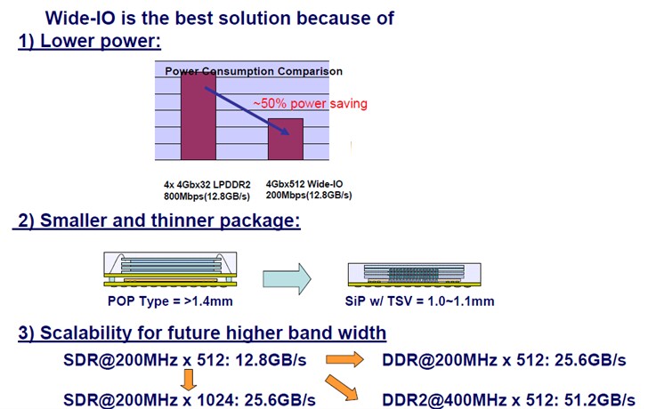
Jim Walker, VP of semiconductor Manufacturing for Gartner during his presentation "Going Vertical" looked at "register DIMM" used in servers comparing the newly announced Samsung 32Gb DDR3 DIMM with through-silicon vias (TSV) to previous 32Gb RDIMM. He finds the TSV-based products operate at lower power and higher speed:

-- Lower power: 4.5 Watts = 30% less than current 32Gb RDIMM without TSV
-- Higher Speed: 1333 Mbit/sec vs. 800 Mbit/sec previous 32Gb RDIMM

Eric Beyne of IMEC sees the current market divided into the following segments:

Mobile consumer applications

Memory/logic stacks:
- Increased memory bandwidth, low power
- Analog-logic stacks: Heterogeneous technology choices

High-performance applications:
- Very high memory bandwidth requirement
- Very high power processor devices
    3D SI interposer substrates

High density memory stacks:
- High bandwidth, low power DRAM

Microsystem integration:
- Combining advanced logic and memory technologies with heterogeneous device technologies such as analog, sensor, actuator, MEMS

Beyne concludes that it is difficult for designers to actually use the technology due to too many unknowns, and lack of 3D-EDA. The numerous technology options create a complex supply chain and make it difficult for equipment, material and EDA tool suppliers to develop the appropriate solutions. Thus, Beyne indicates that standardization is needed immediately in: 3D technology, 3D test, and 3D design.

Roger Hwang, director of test at ASE, noted that test must be built into the 3D TSV assembly flow at the OSAT.


At ASE, logic die will be tested after being mounted onto the substrate "strip" before singulation, and memory will be tested after tape and reel. Another test will be done to the final package after chip-to-chip bonding.


Interposer test will be done after backside processing and after film frame mounting.


Greg Smith of Teradyne listed the following unique TSV fault types:

Faults can occur in the TSV itself:
  • Voids (High resistance)
  • Oxide pinholes (short to substrate)

Faults can occur from bonding:
  • Contamination of bond surface
  • Misalignment
  • Height variation
  • TSV shorts

Faults can occur from wafer thinning:

  • I-V degradation
  • Shifts in device performance

For all the latest in 3D IC and advanced packaging stay linked to IFTLE.........

Monday, September 19, 2011

IFTLE 67 2011 Semicon Taiwan SiP Global Summit: 3D Technology part 1

The SiP global summit was held recently at 2011 Semicon Taiwan in Taipai. It consisted of the 3D IC Test Forum "Test Challenges and Solution in the New Era of Heterogeneous Integration" chaired by Mike Liang, President and CEO, KYEC; the 3D IC Technology Forum, "Embracing the Era of 2.5D & 3D ICs" chaired by Dr. Ho-Ming Tong, GM and chief R&D officer, ASE Group; and the Embedded Substrate forum, "Bridging the Last Mile of Heterogeneous Integration" chaired by Dr. Kuo-Ning Chiang, Professor, director, Advanced Packaging Research Center, NTHU.

Chairman Tong stood by the prediction he made at last year's meeting that serious commercialization of 2.5D and 3D ICs would likely begin in 2013.

Takayuki Watanabe, VP of Elpida's TSV packaging development group, gave a detailed presentation entitled "TSV Technology for 3D DRAM." He described TSV production flow in Elpida where DRAM production and thinning is done in Hiroshima and stacking and assembly in Akita-Elpida.


Their memory stacking process flow is shown below:


In July Elpida announced sampling of their 8Gb DDR3 SDRAM [see "Elpida begins sampling 8Gb DDR3 SDRAM"]. The device is a "low power 8Gb DDR3 SDRAM that consists of four 2Gb DDR3 SDRAMs fitted to a single interface chip using TSV." Elpida believes that the new devices in notebook PCs will demonstrate a 20% reduction in operating power and a 50% reduction in standby power compared with systems that use the standard SO-DIMM configuration. Power consumption is reduced because the TSVs shorten the interconnect between the chips, thus reducing parasitic resistance and capacitance. In addition, chip height is decreased and the DIMM socket is eliminated. Chip mounting area is reportedly reduced 70%.

A 16Gb module (consisting of two 4 chip stacks) occupies far less room (11mm × 15mm) than its SODIMM equivalent (67mm × 30mm) Details of the power savings comparison are shown below.


Wide IO memory technology appears to be the future for mobile products mainly because it brings lower power consumption in a smaller, thinner package while being scalable for future bandwidth requirements. JEDEC is currently working to develop standards for such wide IO memory products.


About a year ago Elpida Memory, Powertech Technology (PTI), and United Microelectronics Corporation (UMC), announced a 3-way 3D IC partnership to Elpida had previously announced their partnership with Powertech Technology Inc. and UMC to build 3D chips for the mobile, high-end graphics and computer markets. [see IFTLE 8, "3D Infrastructure Announcements and Rumors"]

In terms of supply chain, Elpida/UMC/PTI propose the following:


In a separate presentation, Scott Jewler, chief engineering, sales & marketing officer for Powertech Technology, showed their prototype line and the state of construction of their high-volume manufacturing facility.

More info from Semicon Taiwan is coming soon. For all the latest in 3D IC and advanced packaging stay linked to IFTLE............................

Saturday, September 10, 2011

IFTLE 66 3M / IBM Seek to Improve Thermal Underfills; TSMC in Back End Packaging, Again

New thermal underfills for 3D chip stacking

Earlier this week 3M and IBM announced that the two companies "plan to jointly develop the first adhesives that can be used to package semiconductors into densely stacked silicon "towers" [...] which will make it possible to build [...] commercial microprocessors composed of layers of up to 100 separate chips." While giving little technical detail, they announced that this proposed program could "potentially leapfrog today’s current attempts at stacking chips vertically" and offer low power solutions for "makers of tablets and smart phones". IBM was quoted as saying that IBM scientists are "aiming to develop materials that will allow us to package tremendous amounts of computing power into a new form factor -- a silicon "skyscraper." The picture that came along with the press release is shown below. It certainly makes it look like the chips are actually being simply glued together, but if this is 3D stacking with TSV then this would be a chips-last solution, and certainly that cannot be done with more than two layers at a time. My assumption was that this was an oversimplification for the non-technical press release.

With the help of 3M and IBM I have made contact with Herve Gindre, division vice president at 3M Electronics Markets Materials Division, and Bernie Meyerson VP of research at IBM, to clarify exactly what is being proposed.

3M’s Gindre indicates that indeed what we are talking about is basically a thermally-enhanced underfill, which he says "will help conduct heat through 3D multichip stacks and/or away from heat-sensitive components circuits." 3M will staff the program in the semiconductor division of its Electronic Market Materials business, which currently provides temporary bonding solutions and CMP consumables to the 3D market place. Gindre points out that 3M will be focusing their "years of commercial experience in composites, nanotechnology, adhesives and thermal interface materials" on the current problem.

IBM will be running the program out of its semiconductor business unit. VP Meyerson declined to share much detail on timing or technology, which is to be expected since the program hasn’t even started. In terms of thermal performance specifications Meyerson offered that "we clearly wish to exceed current thermally conductive adhesive specifications to the point where the newly developed adhesive solutions at worst match those of silicon."

IFTLE will be following any further developments in this interesting program.

TSMC continues to scope out high-end IC packaging opportunities

Digitimes reports that TSMC has undertaken in-house high-end packaging of ICs, produced by its foundry processes, for fabless IC design houses in the US and Europe [link]. This would obviously create competition for Amkor, ASE, SPIL, STATs and other subcontractors.

At the last several TSMC spring Technology Symposia, in Silicon Valley, TSMC announced plans to expand its efforts in IC packaging. [see PFTLE 30, "Foundry TSV are comin’ -- TSMC makes their play for a biggerportion of the pie"] They have been doing wafer bumping, wafer sort, and wafer-level chip-scale packaging on a limited scale for years. At present, the company has two wafer bumping facilities, located in Hsinchu and Tainan. They are expanding their bumping and wafer-level chip-scale packaging technology and have announced copper pillar bump technology on 100μ bump pitch and will be manufacturing silicon interposers with TSV for 3D stacking. TSMC has announced that it is developing the interposers for Xilinx next-generation FPGAs and is in fact bumping them in-house rather than having that done at one of Taiwan's OSATS [see IFTLE 23, Xilinx 28nm Multidie PPGA…" and IFTLE 43, "IMAPS Device Pkging Highights: 3D IC"].

According to that Digitimes report, "fabless IC design houses are willing to have TSMC responsible for front-end foundry and back-end packaging services although TSMC's packaging ASPs are higher than those of IC packaging/testing service providers." They conclude that this is because these fabless IC design houses like the convenience of a one-stop solution and worry about lower yield rates due to outsourced packaging. However, their sources add that "interestingly, so far, no Taiwan-based IC design houses have accepted TSMC's higher quotes for packaging services."

Indications are that TSMC can generate gross margins of 50-60% for foundry services but even with their higher prices only 20-30% for packaging services. Thus some are questioning why they would expend precious equipment capex on the packaging side.

Whatever your take is on this new information, it is clear that TSMC is slowly but surely moving into what was before a clearly defined packaging and assembly space.

Update on Lester Lightbulb and the LED space

Several of you have tried to leave comments on IFTLE 63, "Bidding Adieu to Lester Lightbulb" and one of you was actually peeved enough that you couldn’t, that you contacted our editor Jim Montgomery. Thanks for that, because it exposed a flaw in the new software that appears to be blocking comments. Jim says they are working on it. One issue appears to be my reported price for the EnduraLED 60W equivalent. One reader claims he has found them for $39 and even $19. Jim got interested in this and tells me that he can now find them for both prices in different parts of the country. All I can tell you is that the Home Depot price on the day the blog was written was $47. The one that I now have installed actually cost me $49.99 since I bought it locally (and still have the receipt). Anyway, my point is not that the price would never come down, but rather how far down it had to come to make purchase of this device a good business decision vs the CFLs. Both bulbs are still glowing brightly -- as well they should, well past my lifetime expectancy if I am to take their marketing propaganda seriously.

Two other readers sent me email indicating that my concern over the life expectancy of the components in the bulb were well-placed, and that this certainly was not taken into account by Philips in their lifetime claims. I guess only Philips can answer that question.

For all the latest on 3D IC and advanced packaging stay linked to IFTLE……………………………………..

Saturday, September 3, 2011

IFTLE 65 Samsung’s 32GB RDIMM DDR3, GLOBALFOUNDRIES Packaging Alliance, Ziptronix Licensing News

Samsung Develops 30nm-class 32GB DDR3 for Next-generation Servers, Using TSV Technology

In December of 2010 IFTLE announced “the Era of 3D IC had arrived“ following the commercial announcement by Samsung that is was beginning the mass production of 8 GB DDR3 memory modules based on the SODIMM form factor [ see IFTLE 27, “The Era of 3D IC has Arrived with Samsung Commercial Announcement”].

Samsung has just announced the development of 32 GB DDR3 memory module (RDIMMs) using their 3D TSV packaging technology and their advanced 30 nm 4 Gb DDR3 chips. The modules can transmit at speeds of up to 1,333 Mbps, a 70 percent gain over preceding quad-rank 32GB RDIMMs (operational speeds of 800Mbps). Further, the 32GB-module consumes 4.5 watts of power per hour, reportedly the lowest power consumption level among memory modules in use in enterprise servers.
Samsung has issued engineering samples of its new modules and is currently collaborating with CPU and controller designers to expand support for 3D TSV server modules.

GLOBALFOUNDRIES and Amkor enter Alliance for Advanced Assembly and Test Solutions
GLOBALFOUNDRIES and Amkor have announced that they have entered into a strategic partnership to develop packaging solutions for advanced silicon nodes. Amkor is thus the founding member of GLOBALFOUNDRIES’ new “Global Alliance for Advanced Assembly Solutions”. GlobalFoundries indicates that they expect to strike similar deals with other companies to create a broader alliance of packaging partners.
As we have detailed many times in IFTLE, the move to advanced technology nodes has caused  packaging and interconnect solutions to become increasingly important. Packaging techniques are leading to improvements in performance and power-efficiency as well as reduced costs. IFTLE readers know that the adoption of 3D IC stacking of ICs is increasingly being viewed as an alternative to traditional technology node scaling at the transistor level. It is also clear that the ability to deliver end-to-end solutions such as 3D IC for customers will require such partnerships between foundries and OSATS to better enable supply chain management.

At their recent “Global Technology Conference” [link] Gregg Bartlett, Sr VP of technology and research and development at GLOBALFOUNDRIES noted that “..the market is beginning to crystallize around certain subsets where system designers want to have that [3D IC]capability in hand,  he continues that “…customers will be demanding 3-D chip stacks late in the 28-nm node or early in the 20-nm node… big graphics and networking chips will demand 3-D chip stacks using interposers…mobile apps processors will want 3-D stacks using through silicon vias”. But, he warned, "…the [3-D IC] supply chain is nearly as complex as the technical solutions".[link]
Indeed previous Globalfoundries roadmaps have shown 3D becoming “enabling” post the 32 nm generation.

Ziptronix signs licensing agreement with Sony
Ziptronix, Inc. has announced a licensing agreement with Sony Corporation for the use of Ziptronix’s patents regarding oxide bonding technology for backside illumination imaging sensors.
Ziptronix has been touting their Zibond™ oxide bonding technology for use in backside illumination (BSI) of CMOS image sensors for several years [ see  PFTLE 40, “Backside Illumination (BSI) Architecture next for NextGeneration CMOS Image Sensors]

 A back-illuminated structure minimizes the degradation of sensitivity to optical angle response, while also increasing the amount of light that enters each pixel due to the lack of obstacles such as metal wiring and transistors that have been moved to the reverse of the silicon substrate. Most of the CIS manufacturers have already moved to BIS technology per a recent market study by Yole
Developpment [ see "CMOS Image Sensors Technologies and MArkets - 2010". CMOS BSI sensors BSI sensor technology is being used by Sony and has been announced in video camcorders and digital still camera products by Casio, Nikon, Ricoh, Samsung, JVC and Fujifilm among others. Ziptronix CTO Paul Enquist asserts that their patented ZiBond™ technology, “…enables the industry’s lowest distortion for imaging systems utilizing backside illumination because of the oxide-oxide bond, alternate solutions, such as adhesives, fail to meet the industry need for ultra low distortion.


In December 2010 Ziptronix filed a complaint against TSMC and Omnivision in Federal Court alleging infringement of several Ziptronix low temperature oxide bonding patents [see IFTLE 31, " Oxide Bonding Patent Litigation Has Begun"] .
 With Sony taking a license on the Zibond technology can Samsung, Toshiba, Cannon, Panasonic, Aptina, ST Micro or others who practice BSI  be far behind ?
Ziptronix CEO Dan Donabedian predicts “… todays digital cell phone cameras that feature up to 5
Megapixel cameras can advance to 16 megapixels using Ziptronix’s patented technology” and similar impact will be seen in “…digital still cameras, digital video cameras, automotive sensors and projection systems such as pico projectors”.  Chris Sanders, Dir. of Business Development notes that Ziptronx is currently “…actively engaged with multiple companies across the globe for licensing our technology in the bsi image sensor space” 

For all the latest on 3D IC and advanced packaging stay linked to Insights from the Leading Edge………