GLOBALFOUNDRIES / Tezzaron MWP Run
CMP, CMC and MOSIS have announced a multiproject wafer run for Jan 2011. MOSIS has been known for years as a supplier of prototype IC runs through its global network of foundry partners. CMP is a broker for IC and MEMS low volume production. CMC is a non profit that supports microelectronics and Microsystems R&D in Canada.
The first two tier face-to-face bonded 3D IC run is based on Tezzarons SuperContact technology and GLOBALFOUNDRIES 130 nm CMOS. We had documented Tezzarons activities in 3D IC previously [ see PFTLE 115 "Semi Award Announced for 3-D IC Actvities", 01/26/2010 ]
When asked about customers potentially being hesitant to work at the 130 nm node Bob Patti, CTO of Tezzaron, replied “They all need to do something different past 28 nm to differentiate themselves. Will anyone really start learning 3D at the 28 node node which will cost hundreds of millions of dollars for design or does it make more sense to start at lower cost node ?? We think likely the latter..”
Patti indicates that the multiproject run opens the door to a lot more companies and Universities to do early development capitalizing on the design kits that have already developed. “There is enough interest already to fill 2-3 reticals with parts “ According to Patti “Tezzaron is a arranging for the Si through Global foundries and will do the assembly, the backside metals and Cu bonding “.
Elpida Announces 3D Alliance
By now you have seen the major announcement that Elpida (Japan), UMC (Taiwan) and Powertech Technologies (Taiwan) have formed an “alliance” to speed up the development of 3D chips at the 28 nm node (link).
This makes so much sense in so many ways. Elpida has had several recent announcements indicating a strong desire to be an early player in 3D [ see PFTLE 101 “Optimism vs Reality; Semantics or Lost in Translation”, 10/11/2009; PFTLE 97 “Ginkgo Biloba”, 9/12/2009; “Elpida Preparing for 3D Commercialization” Semiconductor International, 3/30/2010]. UMC, meanwhile has been very silent about their 3D activity except for joining the ITRI Advanced Stacked- System Technology and Application Consortium (Ad-STAC) [ see PFTLE 99 “3D IC at ITRI”, 9/24/2009 ]. UMC certainly needed to get more press for their activities in order to counter the attention being paid to rival TSMC [ see PFTLE 117 “On Copper Diffusion, Gettering and the Denuded Zone” 02/06/2010; PFTLE 110 “3-D ASIP Update: TSMC & the OSATs”, 12/23/2009 ].
Takao Adachi, CTO in charge of new technology development, has stated that ELpida wants to use it’s 3D technology to “expand beyond its DRAM business and supply systems solutions developed by stacking memory with Rf sensor and logic devices that would come from partner companies” [ see “Elpida Preparing for 3D Commercialization” Semiconductor International, 3/30/2010]. This announcement brings those goals closer to reality. Memory on Logic will enable a large number of I/O between logic and DRAM which increases the data transfer rate and reduces power consumption. Such products will be based on UMC’s foundry logic, Elpida’s DRAM and Powertechs assembly technology.
DIGITIMES reports that PTI has been discussing TSV technology with Elpida for several years and it is speculated that this alliance could lead to a partnership arrangement in the future [ link].
UMC’s CTO reports they expect to be sampling 3D IC solutions using their 28 nm process technology “in mid 2011, with production slated for 2012”
To meet this tight time line IFTLE boldly predicts that 3D interposers it will be used to mate the UMC logic to the Elpida memory. Recall Elpida has extensive background on interposers from their previous work with NEC. [ see PFTLE 28 “NXP Proposes Passive Integration in 3D IC Stacks”, 04/13/2008 ] We will see what really happens shortly. You can be sure you will see updates in IFTLE.
IEEE International 3D Test Workshop
PFTLE has previously listed 3D Test as one of the “4 Horseman” [ see PFTLE 102 The Four Horseman of 3-D IC Integration, 10/14/2009]. The need for standardized 3DIC test protocols have also been documented [ see: PFTLE 108, Testing 3D IC, 12/07/2009 ]
It is therefore with pleasure that IFTLE brings to your attention the 1st IEEE workshop on testing 3D Integrated Circuits “3D – Test” It will be held in conjunction with ITC (Int Test Conf) Nov.2010 in Austin. Check out this site for further details [link]
Leti 300 mm line
Leti has announced that it has opened a complete 300 mm fab extension dedicated to 3D applications. Equipment instillation will continue through the end of the year and an inaugural event is planned for Jan 2011. The line includes lithography, metallization, etching, dielectric dep, wet etch and packaging which will be available for Leti customers and partners.
IBM- the Rumors
In IFTLE 2 “Adv Pkging at 2010 Las Vegas ECTC”, June 2010, I reported the speculation that a TSV containing product would be introduced into their server line. According to the rumor, the product would come off the R&D line.
There are also multiple reports that that you should be aware of, IBM will divest its fab business entirely. On May 11th EE Times reported that “rumors were rampant” that the IBM Microelectronics Division was once again up for sale and that GlobalFoundries was the reported suitor. Boris Petrov, former director of strategic marketing for Chartered has reported [link] that the IBM hardware business currently accounts for ~ 10% of their yearly income. He sees IBM selling their fabs to Globalfoundries (backed by Abu Dhabi finances) and retaining their R&D operations. Under his scenario IBM would provide process and materials engineering for the worldwide GlobalFoundries fab operation. More if these rumors continue to develop.
For all the latest on 3D IC and advanced packaging stay linked to IFTLE.......
remember – for access to all the previous issues of PFTLE go to www.PFTLE.net
Friday, July 23, 2010
Sunday, July 18, 2010
IFTLE 7 Stacking Chips in Vegas
...Finishing our look at 3D IC papers at the 2010 ECTC in Las Vegas.
IBM
Various approaches have been studied and reported to debond the thinned wafer from the mechanical carrier wafer including thermal release, chemical dissolution and laser ablation. The laser ablation method utilizes a glass handle wafer and can be performed at room temperature for a wide range of polymeric adhesives that have proper bonding and absorption characteristics. Using controlled laser ablation parameters, IBM reports that a 200mm wafer can be debonded after a single ablation pass for less than 1.5 minutes.
IBM / TOK
The TOK Zero Newton temporary bonding process has been discussed previously [ see PFTLE 77, Temporary Bonding for 3D Thinning and Backside Processing, May 25 2009] .
IBM and TOK have now examined the use of TOK temporary adhesives with 280 ◦C thermal stability in the TOK Zero Newton wafer handling system. They find that both a high Tg and a high softening point are necessary for thermoplastic temporary adhesives. Materials with low softening point reportedly result in as high as 13 µm “rippling” (localized wafer bow) between the die which makes backside processing “..difficult to impossible”. The new adhesive shows a Tg of 168 ◦C and a softening point of 270 ◦C which results in stability at 280 ◦C for > 1 hr and measured rippling of ~ 0.48 µm.
Temperature stability of 280 ◦C is reportedly required to sustain exposure to backside processing such as PECVD, PVD and solder reflow. It is well known that the quality of plasma deposited SiO2 degrades as processing temperatures are reduced. No off-gassing is seen from this material below 300 ◦C.
The TOK system is debond by a solvent dissolution process through a perforated carrier wafer, i.e. the thinned wafer is mounted on a film frame with the carrier perforations facing upwards, the debonding tool head is aligned with the handler and solvent is injected through the perforated carrier to gently dissolve the adhesive. Once the carrier wafer is removed, the thinned wafer on film frame is rinsed with solvent, washed and spun dry. Disolution rate is reported to be ~ 80 nm/sec.
Full 3D TSV process integration ( the full IBM process sequence for W TSV as IBM previously described in the 2006 ECTC) was carried out to show process efficacy.
CE Leti & ST Micro
Leti and ST Micro have studied the TEOS oxide deposition process in order to control parasitic capacitance for high frequency (1GHz) applications.


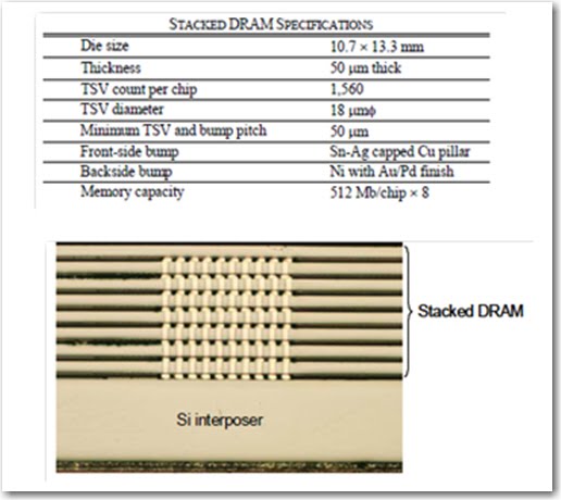
The form factor for memory in mobile devices is limited, therefore there is strong demand for stacked die packaging use TSV to achieve improved performance, increased operating speed and minimum volume. Eliida, Oki and NEC have previously described a stacked DRAM using poly Si TSV [PFTLE 87 NEC points to Ni for Memory 3D TSV, 07/19/2009] but their high resistance interface to the back contact has limited commercialization. We have also reported that in response to these performance issues, NEC has developed electroless Ni v/ immersion Au (ENIG) process for TSV [PFTLE refs] In this ECTC publication NEC details their vias last (backside ) TSV process.
Ni was selected as the plating material because it has a high plating rate (10 to 20 µm/h) and forms a barrier against Sn-Ag solder. W was chosen as the pad metal. Thermal annealing was required to obtain sufficient adhesion to both Si and W interfaces. TSV X-sect are shown in the fig below. Layers are stacked with Cu/(SnAg) bumps. Ni bump height uniformity was an issue that had to be closely monitored. Ni TSV were 0.14 Ω vs previous results for poly silicon which were 4.1 Ω.
Stacked DRAM are shown in the fig below. No indication of commercialization was given.


Fraunhoffer IZM / NEC Schott / Schott Elect Pkging
Michael Toepper and the IZM Berlin group working with Electronic Packaging & Schott GmbH have examined the feasibility of glass interposers. They have focused on W plugs sealed into glass wafers. Rerouting metal is electroplated Au or Cu on a adhesion layer of TiWAu. Bump UBM is deposited TiW/Cu/Ni/Au. Solder balls are attached by ball drop. The higher thermal resistance of glass vs Si means thermal issues will have to be carefully watched.
For all the latest on 3D IC integration and advanced packaging stay linked to IFTLE……………..
IBM
Various approaches have been studied and reported to debond the thinned wafer from the mechanical carrier wafer including thermal release, chemical dissolution and laser ablation. The laser ablation method utilizes a glass handle wafer and can be performed at room temperature for a wide range of polymeric adhesives that have proper bonding and absorption characteristics. Using controlled laser ablation parameters, IBM reports that a 200mm wafer can be debonded after a single ablation pass for less than 1.5 minutes.
IBM / TOK
The TOK Zero Newton temporary bonding process has been discussed previously [ see PFTLE 77, Temporary Bonding for 3D Thinning and Backside Processing, May 25 2009] .
IBM and TOK have now examined the use of TOK temporary adhesives with 280 ◦C thermal stability in the TOK Zero Newton wafer handling system. They find that both a high Tg and a high softening point are necessary for thermoplastic temporary adhesives. Materials with low softening point reportedly result in as high as 13 µm “rippling” (localized wafer bow) between the die which makes backside processing “..difficult to impossible”. The new adhesive shows a Tg of 168 ◦C and a softening point of 270 ◦C which results in stability at 280 ◦C for > 1 hr and measured rippling of ~ 0.48 µm.
Temperature stability of 280 ◦C is reportedly required to sustain exposure to backside processing such as PECVD, PVD and solder reflow. It is well known that the quality of plasma deposited SiO2 degrades as processing temperatures are reduced. No off-gassing is seen from this material below 300 ◦C.
The TOK system is debond by a solvent dissolution process through a perforated carrier wafer, i.e. the thinned wafer is mounted on a film frame with the carrier perforations facing upwards, the debonding tool head is aligned with the handler and solvent is injected through the perforated carrier to gently dissolve the adhesive. Once the carrier wafer is removed, the thinned wafer on film frame is rinsed with solvent, washed and spun dry. Disolution rate is reported to be ~ 80 nm/sec.
Full 3D TSV process integration ( the full IBM process sequence for W TSV as IBM previously described in the 2006 ECTC) was carried out to show process efficacy.
CE Leti & ST Micro
Leti and ST Micro have studied the TEOS oxide deposition process in order to control parasitic capacitance for high frequency (1GHz) applications.


TEOS based SiO2 is deposited by PECVD. The deposition temperature is 260°C due to the thermal instability of the adhesive layer between the temporary carrier and the bonded membrane for temperatures above 250-300°C. The target specifications were a dielectric constant of 4.5, a leakage current below 5 x10⁻⁸ A/cm2 at 2MV/cm and a conformality sufficient to ensure the continuity of the insulation layer at the bottom of the TSV.
O2/TEOS ratios between 0.5 and 8 were examined . The density of the deposits were (surprising to IFTLE ) all identical. The effect of gas ratio on dielectric constant and leakage current are shown below.
The impact of gas ratio on permittivity is significant. As seen in the figure below the mean value of the Dk for the SiO2 deposit strongly decreases with the gases ratio, from 10.81 for a ratio of 0.5 to 4.56 for a ratio of 8. This is associated to the reduction of –SiOH, -SiH and –OH groups in the deposit film as evidenced by FTIR analysis. Only the O2/TEOS ratio of 8 results in an acceptable leakage current of 5.1 x10⁻⁸ A/cm2.

NEC
The form factor for memory in mobile devices is limited, therefore there is strong demand for stacked die packaging use TSV to achieve improved performance, increased operating speed and minimum volume. Eliida, Oki and NEC have previously described a stacked DRAM using poly Si TSV [PFTLE 87 NEC points to Ni for Memory 3D TSV, 07/19/2009] but their high resistance interface to the back contact has limited commercialization. We have also reported that in response to these performance issues, NEC has developed electroless Ni v/ immersion Au (ENIG) process for TSV [PFTLE refs] In this ECTC publication NEC details their vias last (backside ) TSV process.
Ni was selected as the plating material because it has a high plating rate (10 to 20 µm/h) and forms a barrier against Sn-Ag solder. W was chosen as the pad metal. Thermal annealing was required to obtain sufficient adhesion to both Si and W interfaces. TSV X-sect are shown in the fig below. Layers are stacked with Cu/(SnAg) bumps. Ni bump height uniformity was an issue that had to be closely monitored. Ni TSV were 0.14 Ω vs previous results for poly silicon which were 4.1 Ω.
Stacked DRAM are shown in the fig below. No indication of commercialization was given.

Michael Toepper and the IZM Berlin group working with Electronic Packaging & Schott GmbH have examined the feasibility of glass interposers. They have focused on W plugs sealed into glass wafers. Rerouting metal is electroplated Au or Cu on a adhesion layer of TiWAu. Bump UBM is deposited TiW/Cu/Ni/Au. Solder balls are attached by ball drop. The higher thermal resistance of glass vs Si means thermal issues will have to be carefully watched.
For all the latest on 3D IC integration and advanced packaging stay linked to IFTLE……………..
Sunday, July 11, 2010
IFTLE 6 Copper-Copper and IMC Bonding
.............before we begin I wanted to let you know that the PFTLE web page is now up at http://www.pftle.net/. Go there and look around. All of the 128 previous blogs are now accessable, printable and searchable. More on that in the next blog................
Metal-metal bonding at the 2010 ECTC
A few weeks ago I promised to eventually bring you back to more detail on all the copper bonding studies presented at the 2010 ECTC. The categories I will include here are thermocompression Cu-Cu bonding, direct Cu bonding and IMC (intermetallic compound) formation (usually Cu-Sn-Cu bonding).
M-M direct bonding continues to be of significant interest since it is known that it is scalable as evidenced by the SOITEC SOI process which has been in mass production for a decade.
RTI Int
Research Triangle Institute detailed their study on IMC (Cu-Sn-Cu) bonding and Cu-Cu thermocompression bonding. Cu/Sn and Cu strata ready to be mated are shown in the fig below.

The RTI group is comfortable with 20 um pitch features. Anything below that and they saw slippage and subsequent misalignment when the interfaces were brought into contact. (It is felt that this is an equipment limitation not a technology limitation.) Author Reed commented that the plating of 5 um pillars “..requires very good control of the grain structure of the Sn” The Sn surface was flattened using an in situ coining process at 40 Kgf. The copper surface roughness they achieved for various processes is compared in the Table below.
 During the Si recess process IMEC warns that Si etching with SF6 or SF6/O2 results in a highly corroded Cu surface (the protruding nail head). Addition of CF4 was necessary to achieve an acceptable Cu surface. This Cu must then be passivated (i.e Arch MS6020) in order to avoid oxidation during the thermo-compression process.
IMEC also provided further details on their Cu/Sn IMC bonding process. IMEC draws a distinction between processing done above (termed TLP) or below (termed SMB) the melting point of the Sn. When it comes to pressure (compression) requirements, TLP requires far less pressure since the molten Sn makes up for surface irregularities whereas the SMB requires higher pressure . The average roughness of their Cu and Sn plated bumps are 200 and 500 nm respectively. Peak-to valley measurements are even more revealing ( 900 and 2000 nm respectively). The rough bumps prevent Cu and Sn from having good contact and the subsequent inter-metallic formation. Therefore, bonding pressure becomes an important parameter. In fact there is a lower-limit pressure of about 20 MPa below that there is electrical connection lost. However, 150 MPa is almost the upper limit beyond which too much Sn
squeezes out leading to electrical short. Therefore, IMEC chose 50 MPa as a baseline process.
When it comes to pad cleaning NUF (no flow underfill with fluxing additives) was found to work best
CEA Leti
Lea Di Cioccio and her co-workers at CEA Leti continue reporting on their Cu-Cu direct bonding studies [ see PFTLE 58 "Fisk, Buckner and Pasta on the North End", 12/31/2008 and PFTLE 26 "3D Practitioners Assemble at Ft McDowell", 03/23/2008]
They define direct bonding as a process by which two mirror-polished wafers are put into contact and held together at room temperature by adhesive forces, without any additional materials.
Using test vehicles devised at NIST, their extensive electrical measurements show that the direct bonding has negligible effect on the electrical resistance of the structures they have fabricated. Daisy chains of hundreds to tens of thousands of connections were tested and showed a resistance of 79.5 milli ohm per node (bonding interface + copper lines) and a specific contact resistance of the bond ~ 22.5 milli ohm / um sq was extracted.
Their detailed study of the Cu-Cu direct bonded interface reveals a 4 nm CuO interfacial layer which begins to coalesce after 2 hrs anneal at 200 ◦C where CuO is known to become thermodynamically unstable. After a 2 hr 400 ◦C anneal the bonding interface has materials properties very close to native copper.
Metal-metal bonding at the 2010 ECTC
A few weeks ago I promised to eventually bring you back to more detail on all the copper bonding studies presented at the 2010 ECTC. The categories I will include here are thermocompression Cu-Cu bonding, direct Cu bonding and IMC (intermetallic compound) formation (usually Cu-Sn-Cu bonding).
M-M direct bonding continues to be of significant interest since it is known that it is scalable as evidenced by the SOITEC SOI process which has been in mass production for a decade.
RTI Int
Research Triangle Institute detailed their study on IMC (Cu-Sn-Cu) bonding and Cu-Cu thermocompression bonding. Cu/Sn and Cu strata ready to be mated are shown in the fig below.
The RTI group is comfortable with 20 um pitch features. Anything below that and they saw slippage and subsequent misalignment when the interfaces were brought into contact. (It is felt that this is an equipment limitation not a technology limitation.) Author Reed commented that the plating of 5 um pillars “..requires very good control of the grain structure of the Sn” The Sn surface was flattened using an in situ coining process at 40 Kgf. The copper surface roughness they achieved for various processes is compared in the Table below.
 Bonding was performed under a pressure of 5X10ee6 kg/msq for 3 min at 275 to 300 ₀C. Intermetallic phases at the bondline were identified by EDS as Cu3Sn. There was no Cu6Sn5 or unreacted Sn in the bond.
The Cu/Sn-Cu devices with underfill were subjected to 100 thermal cycles (+125°C to -40°C), re-probed, and then 100 hours of 85% RH / 85°C stress testing and re-probed. There were no significant changes in the electrical yield or channel resistance after thermal cycling. The average resistance was 156 Ω before and after stress testing.
Cu-Cu bonding was performed similarly at 325 ₀C and a pressure of 32.2 Kgf for 15 min. The Cu-Cu process was sensitive to any Cu dishing during the CMP with corner and edge pillars showing the most impact. During the bonding process CuO formed on the exposed Cu surfaced in the gap. Chains gave a resistance of 95.9 mΩ.
Die shear strength for both samples was ~ 8kg. For this die size, the 1x shear strength specified in MILSTD- 883E is 2.5kg. Failure occurred at the bond interface
Samsung
Samsung is one of the companies we are following closest in roder to determine the commercial progress of 3D IC. [ see PFTLE: PFTLE 122 "3-D IC at the IEEE ISSCC", 3/12/2010 and PFTLE 116 "Samsung 3-D IC Roadmap" , 02/01/2010]. At the 2010 ECTC, Samsung reported on their studies to determine the best Cu/Sn D2W (die to wafer) bonding approaches. Their test vehicle is shown in the figure below. The pads on the bottom die were Ni/Au rather than Cu. Pads are on 40 um pitch.
 They examined 4 bonding schemes: (1) thermocompression (TC) with profiled heating on the bond tool and bond stage; (2) TC with constant heating on the bond tool and bond stage ; (3) fluxless local reflow bonding ( microscrubbing) and (4) flux bonding.
For TC bonding they found that bump height uniformity, TTV (total thickness variation) and wafer warpage played an important role.
1. TC Profiled heating (i.e. keeping the bonding head <>
IBM
The IBM group notes that Cu-Cu bonding is preferred due to low resistance and superior heart conduction but that high temperature and high co-planarity are needed and that there are alignment problems due to shifts caused by thermal expansion during the joining of these very small features.
Nanyang Univ & GLOBALFOUNDRIES
Nanyang Univ continues to study the use of a self assembled monolayer, SAM (i-hexanethiol) to protect copper surfaces during the Cu-Cu bonding process [ see PFTLE 103 "Show Me the Copper !", 10/23/2009 ]. Upon absorption of the SAM, the Cu surface roughness is reduces from 1.96 nm to 1.55 nm. The SAM can be desorbed from the Cu surface at ~ 200 C. While there is evidence that there is indeed Cu grain growth when samples are bonded at 250 C (vs the control without SAM) the process does not yet look ready for prime time. Unless such a process significantly decreases the surface roughness requirements of TC bonding, one appears better of using a direct bonding process.
IMEC
IMEC reported on their thermo-compression Cu-Cu bonding process for their standard Cu nails process.
The 5um diameter TSVs are etched through the PMD. A thick Ozone-TEOS SiO2 liner is conformally deposited in the TSV holes in order to isolate the TSVs from the Si bulk and to reduce the capacitive coupling. The TSVs are filled with Cu by plating and the Cu overburden is removed by CMP. Finally before final passivation, a Cu layer is added in order to connect the TSVs to the BEOL interconnect. Subsequently the wafer is mounted on a temporary carrier and thinned down to a Si-thickness of ~25 μm by a combination of grinding and CMP. At the end of this sequence, the copper of the TSVs is exposed on the wafer backside. Next the Si is recessed ~700nm by dry etching the Si with respect to the copper TSV. The result of this process is the 10μm pitch Cu nails structure shown in the figure.
 In conventional Cu Back-end technologies this anneal is introduced after CMP in order to soften the Cu (through recrystallization) and thus reduce the CMP time and slurry consumption to remove the Cu overburden. However, due to the large relative dimensions of TSV, built up stress causes large Cu hillock growth from Cu TSV during the anneal at 420ºC after CMP. These protrusions are a potential threat to the IC interconnects layer, especially in case of low-k integration. This copper pumping has been discussed previously [ see PFTLE 103 "Show Me the Copper ! ", 10/23/2009 and PFTLE 125 "3D IC at Ft McDowell", 03/27/2010]
IMEC has shown that CMP of these extrusions after 20 min at 420 ◦C (in forming gas) anneal, will eliminate the protrusions from forming again during any subsequent anneals or high temperature processes.
During the Si recess process IMEC warns that Si etching with SF6 or SF6/O2 results in a highly corroded Cu surface (the protruding nail head). Addition of CF4 was necessary to achieve an acceptable Cu surface. This Cu must then be passivated (i.e Arch MS6020) in order to avoid oxidation during the thermo-compression process.IMEC also provided further details on their Cu/Sn IMC bonding process. IMEC draws a distinction between processing done above (termed TLP) or below (termed SMB) the melting point of the Sn. When it comes to pressure (compression) requirements, TLP requires far less pressure since the molten Sn makes up for surface irregularities whereas the SMB requires higher pressure . The average roughness of their Cu and Sn plated bumps are 200 and 500 nm respectively. Peak-to valley measurements are even more revealing ( 900 and 2000 nm respectively). The rough bumps prevent Cu and Sn from having good contact and the subsequent inter-metallic formation. Therefore, bonding pressure becomes an important parameter. In fact there is a lower-limit pressure of about 20 MPa below that there is electrical connection lost. However, 150 MPa is almost the upper limit beyond which too much Sn
squeezes out leading to electrical short. Therefore, IMEC chose 50 MPa as a baseline process.
When it comes to pad cleaning NUF (no flow underfill with fluxing additives) was found to work best
CEA Leti
Lea Di Cioccio and her co-workers at CEA Leti continue reporting on their Cu-Cu direct bonding studies [ see PFTLE 58 "Fisk, Buckner and Pasta on the North End", 12/31/2008 and PFTLE 26 "3D Practitioners Assemble at Ft McDowell", 03/23/2008]
They define direct bonding as a process by which two mirror-polished wafers are put into contact and held together at room temperature by adhesive forces, without any additional materials.
Using test vehicles devised at NIST, their extensive electrical measurements show that the direct bonding has negligible effect on the electrical resistance of the structures they have fabricated. Daisy chains of hundreds to tens of thousands of connections were tested and showed a resistance of 79.5 milli ohm per node (bonding interface + copper lines) and a specific contact resistance of the bond ~ 22.5 milli ohm / um sq was extracted.
Their detailed study of the Cu-Cu direct bonded interface reveals a 4 nm CuO interfacial layer which begins to coalesce after 2 hrs anneal at 200 ◦C where CuO is known to become thermodynamically unstable. After a 2 hr 400 ◦C anneal the bonding interface has materials properties very close to native copper.

After a 2 hr 200 ◦C post bonding anneal bonding energy is found to be 1.14 J/m2 which is strong enough to sustain post bonding processing such as thinning. After 2 hrs at 400 ◦C a bond energy of 6.6 J/m2 was measured.
The Leti group has also examined the possibility of tungsten-tungsten direct bonding . As deposited by CVD, the W surface roughness is measured at 20 nm which is unacceptable for direct bonding. W CMP was able to bring the RMS roughness down to 0.4 nm. However, W-W bond energy , measured after 2 hr anneals at various temperatures showed very weak bonding had occurred as shown in the fig below. Even at 800 ◦C the bond energy has only reached 1.5 J/m2. Clearly this process is not yet as effective as the Cu-Cu direct bonding process.
 SEMICON
- I'll be at Semicon next week gathering new information for you
Tues June 13th AM I'll be on the panel at TechXSPOT "Bridging the Gap"
Tues June 13th PM I'll be at the Suss workshop "3D Bonding and Thin Wafer Handling"
Wed June 14th PM I'll be at the Alchimer workshop "TSV Metallization that Cost 80% Less"
Hope to see a lot of you at the Sematech reception on Wed night.
For all the latest on 3-D IC and advanced packaging stay linked to Insights From the Leading Edge, IFTLE……..
Tuesday, July 6, 2010
IFTLE 5 2010 Date in Dresden
Design Automation and Test Europe (DATE) was recently held in Dresden. You may recall, last year DATE held a major track on 3-D integration [ see PFTLE 75, “Nice DATE”, 05/09/2009] . Chairs Marinissen, Guillou and Van der Plas repeated the track this year with similar excellent results.

ITRI
We have recently covered 3D activities at ITRI. [see PFTLE 99, "3D IC at ITRI”,
09/24/ 2009 and PFTLE 105, “Taiwanese Focus on 3D “, 11/06/2009 ]
At the 2010 DATE Cheng-Wen Wu from ITRI gave a plenary presentation on “What We Have Learned from SOC Is What Is Driving 3D Integration” Wu reiterated what we have seen previously [ see PFTLE 121 “IC Consolidation, Node Scaling and 3D IC”, 03/03/2010 ] in terms of cost becoming a major obstacle in order to moving forward with future nodes.

When looking at the techniques being developed to ensure 3-D yield, the following slide is a great pictorial to how 2/4 redundancy gives much better odds of yielding a 3D stacked structure than simple TSV doubling.

Synopsys
At Semicon 2009 Ric Borges of Synopsys reported that Synopsys was ramping to provide tools in time for market adoption of 3D IC integration. [ see PFTLE 90 “MCA Delivers 3D Brightspot at Semicon”, 7/31/2009.
At DATE Min Ni of Synopsys examined the role of thermal TSVs in a 3DIC chip stack. When comparing thermal TSV vs fluidic channels they conclude:
Thermal vias & thermal TSVs
– Pros
• can utilize existing vias and TSVs
• no additional processing steps needed
– Cons
• non-scalable due to vertical heat path.
• area penalty for extra thermal TSVs
Fluidic channels
– pros
• scalable with chip area and number of tiers
– cons
• design complexity
• reliability
• needed vertical resources
They ask the question of whether extra TSV are really needed for thermal reasons and if so when should they be added since the thermal hot spots are really not known until the routing is complete.
When looking at Impact of signal/power TSV array on temperature of 3D IC
they conclude that the maximum temperature decreases as TSVs are inserted, however, the effects saturate quickly. The proximity of thermal TSV arrays to hot spots is more critical than array size. For close proximity arrays size matters but benefits from increased array size saturates quickly. It is best to place thermal TSVs in array format to minimize area penalty, close to hotspot to maximize heat conduction. It is the boundary heat transfer coefficient that dictates the steady state temperature of chips, not the amount of TSVs.
 Cascade Microtech
Thomas Thärigen of Cascade Microtech examined “3D IC Test Challenges
and Probing Concepts”. He concludes that 3D IC related DFT (design for test)
Is the key success factor for testing of 3D stacked devices, since contacting 3D circuits has several limitations (see case study later) Without considering test during design phase it will be impossible to perform effective tests on 3D stacked IC’s.
For the bottom wafer:
Probe on Regular Front-side Pads
- Function can be tested
- TSVs can not directly tested
- State of the art contact technology with regular cantilevers:
high alignment speed and high contact stability
- Available for Known Good Die/Stack Test and for Engineering Test
- Can be combined with non contact techniques
- State of the Art design techniques required for testability
- Only for the first tier
Wafer on carrier: thinned and backside completed
Probe on Extra DFT Pads
- State of the art contact technology with regular cantilevers:
high alignment speed and high contact stability
- Available for Known Good Die/Stack Test and for Engineering Test
- Limited number of regular-sized pads must be added by DFT
- Execute RPCT inside die which must be designed in by EDA
- Can be combined with non contact techniques
- Medium probe force vs. adhesive stiffness is currently under investigation
Probe on Micro Bumps
- Challenge: TSV micro-bumps small (e.g. 25μm) & numerous
- Available for KGD/KGD and Engineering Test using vertical probe cards
- Access to high pin counts = high bandwidth for tests
- Normally this TSV contacts are inter-die connects
- DFT is required to have all contacts available to execute test routines for
the single die
- Can be combined with non contact techniques
- High pin count = high probe force: Probe force vs. adhesive
stiffness is currently under investigation
Probe on TSV’s
- Challenge: TSV’s very small (e.g. 5μm) and numerous
- Only for engineering purpose, no further wafer processing possible
afterwards (bonding does not work due to probe marks)
- Use of small single tips required = only very limited number of
contacts simultaneously
- Design required to implement dedicated engineering test structures
Non contact probing is limited to pitch due to antenna issues.
The complete set of presentations can be found here:
[http://http://www.date-conference.com/conference/date10-workshop-W5
coming soon at IFTLE:
- Copper-Copper and IMC Bonding
- Stacking Chips in Vegas
- 3D IC at the IITC
- taking a look at the new ITRS roadmaps
SEMICON - I'll be at Semicon next week gathering new information for you
Tues June 13th AM I'll be on the panel at TechXSPOT "Bridging the Gap"
Tues June 13th PM I'll be at the Suss workshop "3D Bonding and Thin Wafer Handling"
Wed June 14th PM I'll be at the Alchimer workshop "TSV Metallization that Cost 80% Less"
Hope to see a lot of you at the Sematech reception on Wed night.
For all the latest on 3-D IC and advanced packaging stay linked to Insights From the Leading Edge, IFTLE……..
ITRI
We have recently covered 3D activities at ITRI. [see PFTLE 99, "3D IC at ITRI”,
09/24/ 2009 and PFTLE 105, “Taiwanese Focus on 3D “, 11/06/2009 ]
At the 2010 DATE Cheng-Wen Wu from ITRI gave a plenary presentation on “What We Have Learned from SOC Is What Is Driving 3D Integration” Wu reiterated what we have seen previously [ see PFTLE 121 “IC Consolidation, Node Scaling and 3D IC”, 03/03/2010 ] in terms of cost becoming a major obstacle in order to moving forward with future nodes.
When looking at the techniques being developed to ensure 3-D yield, the following slide is a great pictorial to how 2/4 redundancy gives much better odds of yielding a 3D stacked structure than simple TSV doubling.
Synopsys
At Semicon 2009 Ric Borges of Synopsys reported that Synopsys was ramping to provide tools in time for market adoption of 3D IC integration. [ see PFTLE 90 “MCA Delivers 3D Brightspot at Semicon”, 7/31/2009.
At DATE Min Ni of Synopsys examined the role of thermal TSVs in a 3DIC chip stack. When comparing thermal TSV vs fluidic channels they conclude:
Thermal vias & thermal TSVs
– Pros
• can utilize existing vias and TSVs
• no additional processing steps needed
– Cons
• non-scalable due to vertical heat path.
• area penalty for extra thermal TSVs
Fluidic channels
– pros
• scalable with chip area and number of tiers
– cons
• design complexity
• reliability
• needed vertical resources
They ask the question of whether extra TSV are really needed for thermal reasons and if so when should they be added since the thermal hot spots are really not known until the routing is complete.
When looking at Impact of signal/power TSV array on temperature of 3D IC
they conclude that the maximum temperature decreases as TSVs are inserted, however, the effects saturate quickly. The proximity of thermal TSV arrays to hot spots is more critical than array size. For close proximity arrays size matters but benefits from increased array size saturates quickly. It is best to place thermal TSVs in array format to minimize area penalty, close to hotspot to maximize heat conduction. It is the boundary heat transfer coefficient that dictates the steady state temperature of chips, not the amount of TSVs.
Cascade MicrotechThomas Thärigen of Cascade Microtech examined “3D IC Test Challenges
and Probing Concepts”. He concludes that 3D IC related DFT (design for test)
Is the key success factor for testing of 3D stacked devices, since contacting 3D circuits has several limitations (see case study later) Without considering test during design phase it will be impossible to perform effective tests on 3D stacked IC’s.
For the bottom wafer:
Probe on Regular Front-side Pads
- Function can be tested
- TSVs can not directly tested
- State of the art contact technology with regular cantilevers:
high alignment speed and high contact stability
- Available for Known Good Die/Stack Test and for Engineering Test
- Can be combined with non contact techniques
- State of the Art design techniques required for testability
- Only for the first tier
Wafer on carrier: thinned and backside completed
Probe on Extra DFT Pads
- State of the art contact technology with regular cantilevers:
high alignment speed and high contact stability
- Available for Known Good Die/Stack Test and for Engineering Test
- Limited number of regular-sized pads must be added by DFT
- Execute RPCT inside die which must be designed in by EDA
- Can be combined with non contact techniques
- Medium probe force vs. adhesive stiffness is currently under investigation
Probe on Micro Bumps
- Challenge: TSV micro-bumps small (e.g. 25μm) & numerous
- Available for KGD/KGD and Engineering Test using vertical probe cards
- Access to high pin counts = high bandwidth for tests
- Normally this TSV contacts are inter-die connects
- DFT is required to have all contacts available to execute test routines for
the single die
- Can be combined with non contact techniques
- High pin count = high probe force: Probe force vs. adhesive
stiffness is currently under investigation
Probe on TSV’s
- Challenge: TSV’s very small (e.g. 5μm) and numerous
- Only for engineering purpose, no further wafer processing possible
afterwards (bonding does not work due to probe marks)
- Use of small single tips required = only very limited number of
contacts simultaneously
- Design required to implement dedicated engineering test structures
Non contact probing is limited to pitch due to antenna issues.
The complete set of presentations can be found here:
[http://http://www.date-conference.com/conference/date10-workshop-W5
coming soon at IFTLE:
- Copper-Copper and IMC Bonding
- Stacking Chips in Vegas
- 3D IC at the IITC
- taking a look at the new ITRS roadmaps
SEMICON - I'll be at Semicon next week gathering new information for you
Tues June 13th AM I'll be on the panel at TechXSPOT "Bridging the Gap"
Tues June 13th PM I'll be at the Suss workshop "3D Bonding and Thin Wafer Handling"
Wed June 14th PM I'll be at the Alchimer workshop "TSV Metallization that Cost 80% Less"
Hope to see a lot of you at the Sematech reception on Wed night.
For all the latest on 3-D IC and advanced packaging stay linked to Insights From the Leading Edge, IFTLE……..
Subscribe to:
Posts (Atom)