Sunday, March 31, 2013

IFTLE 141 100GB Wide IO memory; AGC Glass Interposers; Nvidia talks stacked memory

 2013 ISSCC

At the 2013 IEEE ISSCC researchers from Kobe Univ and the ASET group (Assoc. of Super Advanced Electronic Technologies) presented their work on "A 100 GB/s Wide IO with 4096b TSVs through an active silicon interposer with in place waveform capturing."

As shown in the figure below their work constitutes a major jump in both bandwidth and energy consumption from other published work.


The system design is shown below. The wide IO data bus is capable of 100 GB/s sync bidirectional data transfer at 200 MHz. By putting waveform capture on the active silicon interposer (ASIP), they were able to monitor signal and power integrity within the stack. The silicon interposer provided horizontal and vertical routing for the TSV and microbumps.


Further specifications are given in the chart below.
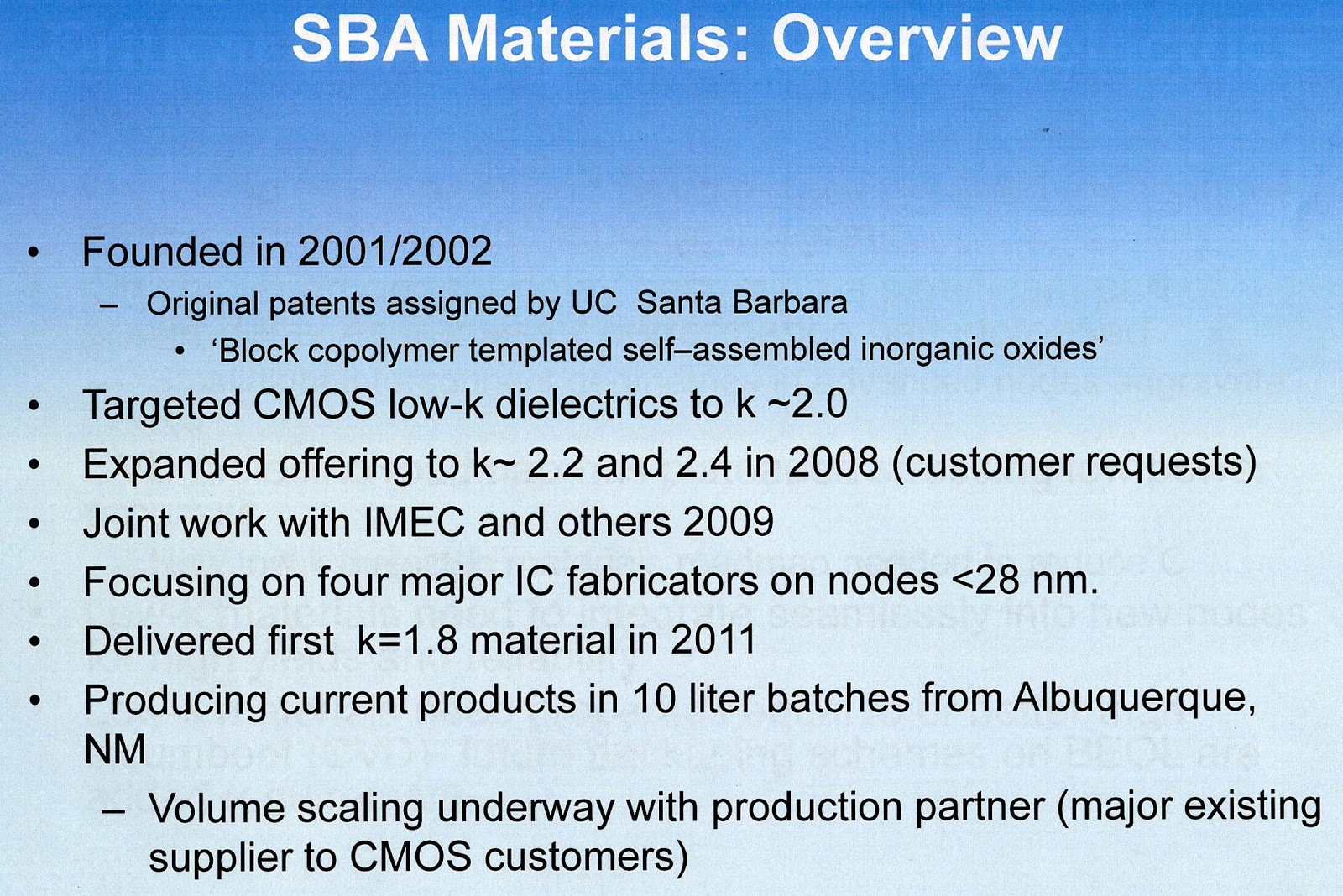


Asahi Glass enters the Glass Interposer Market
Triton then will apply its proprietary technology to fill the high-aspect-ratio via holes with a copper paste that has the same coefficient of thermal expansion as glass.
At Nvidia's annual Graphics Technology Conference last week they announced the Volta, scheduled for release in 2015, will use stacked memories. They see the modules built on  2.5-D interposers since graphics chips generate too much heat to be stacked vertically with memories in a 3D stack.
At the recent IMAPS Device Packaging Conference in Scottsdale, AZ, the big news was that Asahi Glass (AGC) and nMode Solutions had invested $2.1 million to found Triton Micro Technologies to develop glass based 2.5D Interposers. The new company will be headquartered in Tucson AZ with a manufacturing facility planned in CA.

They will manufacture glass interposers using AGC’s EN-A1 alkali-free boro-aluminosilicate glass which has low CTE and thermal expansion properties matched to silicon. EN-A1 reportedly has refractive properties which allow for a low taper when laser drilled, providing for precise pitch control and hole size. EN-A1 has a highly polished surface and can readily accept either thin-film or thick-film metallization directly on the glass without the need for an adhesion layer. Surface roughness of 10 Å or less is typical.
Triton CTO Steve Annas indicated that they are ready for prototyping now.

Nvidia talks GPU + Memory Stacks
In an interview with EE Times [link] Nvidia Chief Scientist Bill Dally reports that the difference between 28 and 20 nm nodes is about 20 to 25 percent "Therefore, process doesn't matter that much anymore. If Nvidia is clever about architecture and circuit design, then can make up for the fact that Nvidia has competitors [Intel] that are a node ahead."    He sees chip stacking as an alternative to moving to the next semiconductor node "at a time when process technology is providing less bang for the buck."
For all the latest in 3DIC and advanced packaging, stay linked to IFTLE...


Sunday, March 24, 2013

IFTLE 140 Important Apple Rumors; Xilinx not Deserting 2.5D; Book to Bill Improving


I’m pushing back reports from the IMAPS Device Packaging Conference a week because the rumors below are timely and, if true, very important

More Apple Rumors

In IFTLE 139 [see IFTLE 139, “ More on Apple A7 processor Production Rumors …”] I reported on a  Digitimes report that TSMC is expected to tape out Apple's A7 processor on a 20nm process in March and then "..move the chip into risk production in May-June, which will pave the way for commercial shipments in the first quarter of 2014… TSMC will utilize 14-fab to manufacture the A7 chips for Apple" and that  "institutional investors" were reporting that  "Samsung is likely to receive 50% of the A7 processor orders, TSMC 40%, and Intel 10%."

What we didn’t discuss was whether TSMC would be filling the order as an 2.5D interposer based module. Over a year ago [ see IFTLE 88 Apple TSV Interposerrumors…] we reported rumors that the A6 was being taped out as an interposer based module. Obviously that didn’t happen 

In response to IFTLE 139 highly placed readers in Taiwan have reported that "A7 will continue to use PoP and will not adopt CoWoS or any other TSV based technology" They report that "slowing down of 2.5D is due to lack of availability of DRAM stack and anticipation of DDR4." Hmmm...

IFTLE has been saying for a long time that MEMORY had to be there first or the rest of these expected application could not move forward.  

IF this report is true, when taken in combination of the comments by ST Ericssons Kimmich [see IFTLE 134, “SEMI 3DEuropean Summit – Is the Wide IO Driver Dead ?”] on the push back for wide IO by DDR4, this is surely a strong 1,2 punch to the gut for 2.5/3D commercialization.

Although Samsung, Hynix, Micron and Elpida have been working on this for a long time, it sounds like maybe we are still not there.

I’m hoping this is pure BS [like the bogus story of Samsung paying their Apple fines in nickels (still smarting from that one)], but this is from people in the know and I felt you should at least be aware of what’s being said behind closed doors. Hopefully we can laugh this off in a few weeks or months when it is proven to be untrue.

Anyone Need CoWoS ?

Other reports from Taiwan indicate that TSMC has done a complete 360 from a few years ago and is now pushing CoWoS and telling customers that they need to adopt NOW if they want to get future priority.

…but it still comes down to - Is the memory ready (meaning technology and cost) ??

Altera and Xilinx returning to PoP

In IFTLE 139, we also shared the Digitimes report that Xilinx and Altera would be shedding 2.5D technology and returning to PoP. My contacts at Xilinx and Altera both denied the statement, and maybe they were telling the truth. Again, well situated personnel in Taiwan report that Xilinx will continue to use silicon 2.5D but that Altera is looking very closely at the use of organic interposers as a lower cost solution.

Semi Book to Bill

Semi just reported a book to bill of 1.10 for Feb 2013, which is good news . The three-month average of worldwide billings in February 2013 was $975.3 million. While this number is  26.3 percent lower than the February 2012 billings level of $1.32 billion, it indicates that we are coming out of the downturn that we were in last fall.

For all the latest on 3DIC and advanced packaging, stay linked to IFTLE.


Sunday, March 17, 2013

IFTLE 139 More on Apple A7 processor Production Rumors ; DARPAs ICECool part 2 – Applications


TSMC / Intel and the  Apple A7 processor

Steve Shen of Digitimes [link] reports that TSMC is expected to tape out Apple's A7 processor on a 20nm process in March and then "..move the chip into risk production in May-June, which will pave the way for commercial shipments in the first quarter of 2014… TSMC will utilize 14-fab to manufacture the A7 chips for Apple."

J Lien & J Chang of Digitimes report rumors from "institutional investors" that "Samsung is likely to receive 50% of the A7 processor orders, TSMC 40%, and Intel 10%." [link]

Altera and Xilinx returning to PoP ?? (I hope Not ! )

Digitimes also reports that according to the Chineese language "Economic Daily News,"  Altera and Xilinx are considering switching to PoP (package on package) technology for their next-generation chips, instead of continuing with TSMCs 2.5D CoWoS process [link]. "Altera and Xilinx are considering switching their packaging orders to Advanced Semiconductor Engineering (ASE) and Siliconware Precision Industries (SPIL) as both plan to ramp up their PoP packaging capacity in 2013," EDN said.  TSMC, ASE and SPIL all declined to comment on market reports, EDN said.
Reportedly yields and cost of trial production using a 20nm production node and the 2.5D CoWoS process at TSMC in past months failed to meet expectations, prompting Altera and Xilinx to seek alternative packaging solutions, said the paper.

 [Highly placed contacts at Xilinx and Altera are denying the veracity of this story and I want to believe them.]  


DARPA ICECool part II - Applications

Military platforms often cannot physically accommodate the large cooling systems needed for thermal management, meaning that heat can be a limiting factor for performance of electronics and embedded computers. DARPA introduced the  interchip/Intra chip enhanced cooling program (ICECool)  in June 2012 to explore ‘embedded’ thermal management. [ see IFTLE 119 “ICECool Puts 3D Thermal issues Back in Focus”]


The premise of ICECool is to bring microfluidic cooling inside the substrate, chip or package, including thermal management in the earliest stages of electronics design. The first track of the program, ICECool Fundamentals, has already begun basic research into microfabrication and evaporative cooling techniques.

Under the new ICECool Applications Track, DARPA seeks demonstration of  microfluidic cooling in (A) monolithic microwave integrated circuits (MMICs) and (B) embedded HPC modules. For part B Proposers are expected to define and explore intrachip, interchip or hybrid approaches compatible with a 2.5D or 3D configuration, such that they would be compatible with DARPA, DoD, and commercial investments and trends in 3D stacking of silicon chips.

DARPA expects proosed approaches for ICECool Applications to involve embedded thermal management through microfluidic heat extraction in close proximity to the primary on-chip heat source(s), aided by heat flow through high conductivity thermal interconnects and/or thermoelectric devices from sub-millimeter “hot spots” to liquid-cooled miniature passages, as conceptualized in the figure below. An intrachip cooling approach would involve fabricating miniature passages directly into the chip. An interchip approach would utilize the microgap between chips in three-dimensional stacks for the cooling.
DARPA further expects proposers to define and demonstrate intrachip and/or interchip thermal management approaches that are tailored to a specific application that are consistent with the materials sets, fabrication processes, and operating environment of the intended application.
Proposers are encouraged to apply their proposed solution to existing liquid-cooled systems, in which the external thermal management hardware can be redesigned into an ICECool design.
In Phase 1 performers will be allowed 12 months to a) design, fabricate, and demonstrate the
feasibility of the proposed ICECool concept with an appropriately configured Thermal
Demonstration Vehicle (TDV) and to b) establish, through electrical-thermal-mechanical co-simulation, the performance enhancement that can be achieved in the targeted electronic module. Performers will be judged based on thermal performance versus the stated thermal metrics, the simulated performance that would be achieved utilizing their thermal strategy, and their ability to adhere to this schedule.
In Phase 2, selected teams will be allowed 18 months to implement and validate their ICECool strategy in an operational Electrical Demonstration Vehicle (EDV) module and demonstrate their ability to simultaneously meet both thermal and functional performance metrics. In both Phase 1 and Phase 2, it is expected that performers will have significant performance and reliability modeling tasks that flow from the preliminary models that are developed as part of the proposal process.
The full solicitation may be found at: http://go.usa.gov/25qx. The ICECool Applications BAA closes March 22, 2013.
For all the latest on 3DIC and advanced packaging, stay linked to IFTLE...

Friday, March 8, 2013

IFTLE 138 Foundry Intel; 300 mm Capacity; SBA Low-K Oxide

Foundry Intel –Altera is the beginning... Is Apple Next?

IFTLE first asked the question "Intel becoming a Foundry?" back in 2011 [see IFTLE 23, "Xilinx 28nm FPGA,Copper Pillar Advances at Amkor and Intel looking at Fab options"] when they entered into an agreement with Achronix Semiconductor. IFTLE ended this segment with the comment "While Intel is brushing this off as unimportant, I would keep an eye out for further developments."


Well, last week Altera and Intel entered into an agreement for the future manufacture of Altera FPGAs on Intel's 14nm tri-gate transistor technology. In what some see as Altera’s attempt shift the headlines from Xilinx 2.5D technology splash of 2011-2012, Altera remarked that "using Intel 14nm technology will enable customers to design with the most advanced, highest-performing FPGAs in the industry," adding that they were "the only major FPGA company with access to this technology" which they feel gives them a significant advantage in "power, performance and density." Altera still plans to use TSMC as its primary foundry but this ends the 20-year dominance of TSMC as Altera's sole foundry.

This could signal the start of more intense competition between TSMC and Intel. Rumors abound that the next Intel target in this potential TSMC-Intel battle would be Apple.

Reuters and Forbes [link]  are reporting that “Intel's next CEO is likely to shepherd the top chipmaker into a growing contract-manufacturing business, a strategic shift that could lead to a deal with Apple Inc and give it a fighting chance to make inroads in the mobile arena. A source close to one of the companies says Intel and Apple executives have discussed the issue in the past year, but no agreement has been reached. Sunit Rikhi, vice president and general manager of Intel custom foundry, told Reuters last week his group is ready to take on a potential large, unidentified mobile customer, although he declined to discuss Apple specifically.[link]


300mm Capacity

Our friends at IC Insights took a look at 300mm wafer capacity leaders and found that half are primarily memory suppliers, two are pure-play foundries, and one company, Intel, is focused on MPUs [Global WaferCapacity 2013—Detailed Analysis and Forecast of the IC Industry’s Wafer FabCapacity].  Samsung was by far the leader in 2012, with about 61% more 300mm capacity than second-place SK Hynix. Intel was the only other company that held a double-digit share of 300mm capacity at the end of 2012.  Assuming Micron is successful in acquiring Elpida in 1H13, the combined 300mm wafer capacity of the two companies will make the merged company the second-largest holder of 300mm capacity in the world behind Samsung. IC Insights expects the largest increase in 300mm capacity to come from the foundries—TSMC, GlobalFoundries, UMC, and SMIC  who are projected to more than double their collective 300mm wafer starts per month by 2017.

More Info on SBA oxide low K


(Click for full size image)

IFTLE has been keeping an eye on startup SBA for several years since they appear to be the only SiO2 dielectric choice for Low K IC chips that can actually deliver on sub 2.5 Dk [see: Low-k dielectric family introduced by SBA Materials]

New President and COO Hash Pakbaz recently presented an update at the IEEE Advanced Packaging Materials Conference in Irvine.
A few key slides are shown below.


(Click to see full size image)

With IFTLE whispering in their ear, they are also beginning to look at 2.5 and 3D as applications suitable for this thick spin on oxide coating.

For all the latest in 2.5, 3D IC and advanced packaging, stay linked to IFTLE.

Saturday, March 2, 2013

IFTLE 137 CMOS Image Sensor Market Update


Yole Developpment recently gave a webinar based on their fall 2012 report on the CMOS Image Sensor Market. For those of you who didn’t attend it, lets look at some of the interesting facts that they presented.

The CIS module value chain can be broken out into segments consisting of front end chip fab, optical layers, back end / packaging and module assembly and test. The figure below shows their estimated market values in 2012.

 
The market is seen evolving...

Revenue by application is shown in the figure below. By 2016, revenue should exceed $10B with mobile handsets and consumer applications, such as accounting for most of that revenue.


In 2011 OmniVision, Samsung and Sony were responsible for 50% of the $5.8B market. Taiwan, Korea and Japan accounting for 80% of the total market.

The low end market segments include cell phones, toys and bar code readers. The evolving high end market segments include medical, DSLR cameras, automotive, machine vision, surveillance etc.
BSI technology will have taken 50% of the overall market by 2015. 

 
The next generation technology will be 3D stacking which is already being introduced by Sony [ see IFTLE 112 "TSMC Staffing up or 2.5/3D expansion; Semi 3D Standards; Sony Shows off 3D Stacked Image Sensors"]


For all the latest in 3DIC and advanced packaging, stay linked to IFTLE.