The importance of of suitable design tools for 3D IC have been detailed previously [ see IFTLE 9 “3D In and Around the Moscone Part 1”, Aug, 2010; PFTLE 102 The 4 Horsemen of 3D IC”,10/16 2009; PFTLE 70 “Deep in the Heart of Texas” 04/04/2009 ].
Well, it’s now becoming clear that significant EDA industry attention is being directed towards 3D IC technology.
The Design Automation Conference (DAC) which started in 1964 is clearly the preimminent technical conference / trade show, specializing in design automation. DAC is sponsored by several professional societies including IEEE Circuits and Systems Society, the IEEE Solid-State Circuits Society and the IEEE Council on Electronic Design Automation. The 2010 DAC was held in Anaheim CA.
This year, 3D IC design finally took a prominent position in the technical program. Rahul Deokar of Cadence called 2010 DAC "...a coming out party for 3D-IC design” (Link). Rick Nelson (Editor –in-chief of Electronic Design News) after attending the 3D activities at DAC writes that “the time is now for 3-D stacked die” and that “the consensus seems to be that the 3-D revolution is imminent.
Every once in awhile someone comes up with something cleaver where I think to myself “damn I wish I had thought of that” So hats off to Rick Nelson for his 3D clock (left). I’m sure I’ll be using this in future slide presentations, so in case I forget to give Rick credit, I’m doing so now in public.

In the first ever DAC panel session dedicated to 3D IC entitled "3D Stacked Die: Now or the Future?" included Myung-Soo Jang of Samsung, LC Lu of TSMC, Philippe Magarshack of ST Micro, Marchal Paul of IMEC and Riko Radojcic of Qualcomm. They all addressed the question "Are we (3D IC) there yet ?...Is it now or the future?"
There was a consensus among the speakers that commercial release of the first 3D memory on logic devices was imminent. (IFTLE feels this is a bit aggressive and continues to support the belief that prototypes may be seen in 2011 but full commercialization will not be seen till 2012)
Lu indicated that TSMC was developing 3D TSV technology with a broad focus on design, packaging and testing as well as the required foundry fabrication process. Lu indicated that n advances in design could help address current challenges related to process variations, thermal and mechanical stress.
Jang noted that design tools that work together seamlessly were required to “...speed the adoption of 3-D implementations”. Jang indicated that online video applications and mobile apps will require as much as 12.8 Gb/sec between I/O and memory with today's IC technology whereas 3-D packaging technology is expected to lower that by ~ 8X in Samsung DDRs.
Radojcic commented that 3D IC is "... not a one size fits all technology” and that it is essential to implement a Path Finding process up front in the system design in order to explore design options and make the right choices with respect to “technology, costs and die interactions”. As he has indicated at several other meetings recently [see IFTLE 11 “3D In and Around the Moscone Part 1”, Aug 2010] Radojcic feels that 3D IC ".. is all about managing choices” .
Marchal called 3D IC IMECs “man on the moon” program due to the long gestation period that was required to get all the necessary technologies into place. He prognosticated that 3D technology would arrive “ in the next two to three years," indicating that the technology has three main application drivers including “...convergence, high performance and memory systems."
DAC also held a tutorial entitled “3-D: New Dimensions in IC Design” which included instruction by Prof. Yuan Xie - Penn State, Prof. David Atienza - EPFL, Switzerland, Tanay Karnik – Intel, Paul Marchal – IMEC and Ruchir Puri - IBM .
As part of the conference the GSA (Global Semiconductor Association) held a 3D forum which reportedly had 125 attendees. Presentations were from major foundries, IDMs, EDA/IP vendors, design services and other industry organizations trying to accelerate 3D design.
For a short video of Lisa McIlrath of R3Logic discussing 3D design and design tools and their design tool “R3 Integrator” you can go here (link) .
The Global Semiconductor Alliance
In 2009 GSA’s EDA Interest Group, with representatives from EDA vendors, semiconductor firms, IC design services, research institutes and others decided to focus efforts on tools and flows to support the rapidly emerging 3-D/TSV technology. In the June 2010 issue of GSA forum, they addressed the benefits of 3D technology and described the results of an industry survey that they did on the subject.
While IFTLE agrees with their conclusion that “Accurate modeling tools and techniques, 3-D process design kits (PDKs), productive planning/partitioning tools, as well as 3-D-aware implementation and verification tools are needed. Design for 3-D testability is another challenge EDA needs to address.” Other comments like “Die stacks interconnected with TSVs are already in volume production (e.g., CMOS image sensors (CIS) in digital cameras and memory chips on top of each other to manufacture larger memory only configurations)” makes IFTLE wonder where they are getting their 3D technology industry status information. Oviously not from PFTLE or IFTLE ! for those readers know that while CIS do use TSV, they do not yet have stacked chips and while memory prototypes have been built with TSV, they are not yet commercial and certainly not is “volume production”
Lets look at some of the interesting survey conclusions that they reported. 36 semiconductor vendors responded. All expressed interest in 3-D/TSVs, and ~ 1/3 reported that they were already involved in ongoing 3-D/TSV R&D efforts. Eight of the 36 respondents are very large IC vendors, mostly fabless or fab-light, focused on the consumer and communications markets, and sell mixed-signal ICs. All achieved more than $1 billion in revenue in 2008. Seven companies generated between $100 million and $1 billion in revenue in 2008, and these companies design and manufacture mostly analog, RF and mixed-signal chips.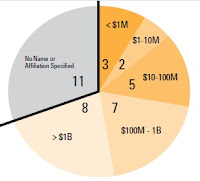


next week Part 3 of 3 concerning 3D activities at Semicon 2010.
For all the latest on 3D IC and advanced packaging stay linked to Insights From the Leading Edge...
Past PFTLE blogs are now available at www.pftle.net............
At the Atrenta booth they conducted live demonstrations of a working 3D design flow. The design flow addresses 3D-aware high-level synthesis, early partitioning, floorplanning and multi-domain analysis. The system is the result of on-going collaboration between Atrenta, AutoESL and Qualcomm.
TSMC and Cadence
In a joint announcement at DAC, TSMC and Cadence announced that Cadence 3D-IC implementation and integrated DFM have been incorporated into TSMC Reference Flow 11.0. (link). ST Juang, senior director of Design Infrastructure Marketing at TSMC noted that . “TSMC Reference Flow 11.0 enables 3D-IC integration to become part of the mainstream flow.” Advanced 3D design capabilities including physical design and implementation; RC extraction; analysis of timing, signal integrity, IR drop, electromagnetic and thermal analysis; and physical verification are included.
With this breakthrough year at DAC, IFTLE concurrs that “The time for 3D time is now !”
The Global Semiconductor Alliance
The Global Semiconductor Alliance was formed in 1994 as the “Fabless semiconductor Association”. Their goal is to focus on initiatives that will contribute to the growth and profitability of the semiconductor industry.
Lets look at some of the interesting survey conclusions that they reported. 36 semiconductor vendors responded. All expressed interest in 3-D/TSVs, and ~ 1/3 reported that they were already involved in ongoing 3-D/TSV R&D efforts. Eight of the 36 respondents are very large IC vendors, mostly fabless or fab-light, focused on the consumer and communications markets, and sell mixed-signal ICs. All achieved more than $1 billion in revenue in 2008. Seven companies generated between $100 million and $1 billion in revenue in 2008, and these companies design and manufacture mostly analog, RF and mixed-signal chips.

Mobile Internet devices (MIDs) are an obvious target segment to benefit from the space, power and cost savings that; 3-D/TSV offers. Cell phones were identified as the primary 3-D/TSV target application. Netbooks, Global Positioning System(GPS)systems and digital cameras were next in popularity.

Performance is the primary motivator for using this technology, while footprint , combined with board space savings, is a close second.

Practically all die stacks will contain at least one layer of memory.

There is also interest in integration of passives into the stack.

For all the latest on 3D IC and advanced packaging stay linked to Insights From the Leading Edge...
Past PFTLE blogs are now available at www.pftle.net............
No comments:
Post a Comment