Chairman Tong stood by the prediction he made at last year's meeting that serious commercialization of 2.5D and 3D ICs would likely begin in 2013.
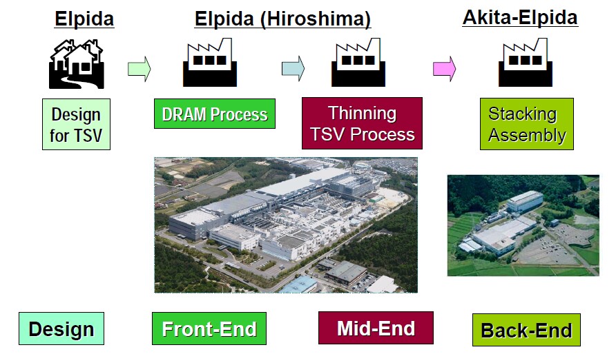
Takayuki Watanabe, VP of Elpida's TSV packaging development group, gave a detailed presentation entitled "TSV Technology for 3D DRAM." He described TSV production flow in Elpida where DRAM production and thinning is done in Hiroshima and stacking and assembly in Akita-Elpida.

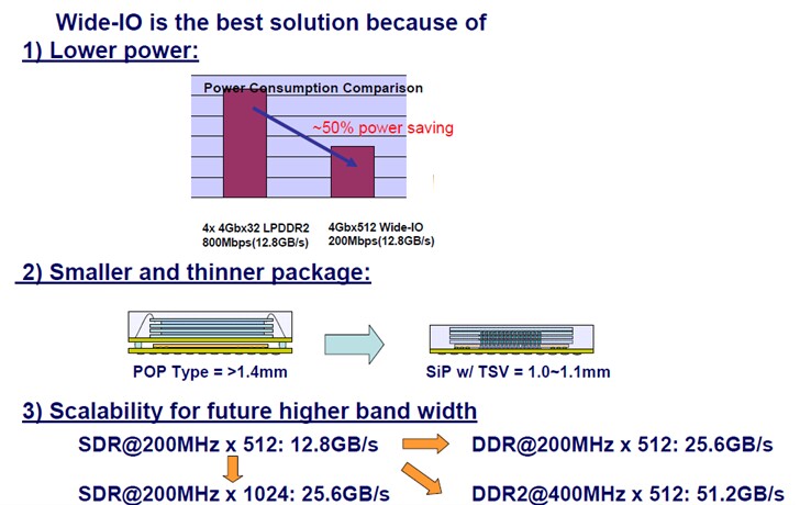
In July Elpida announced sampling of their 8Gb DDR3 SDRAM [see "Elpida begins sampling 8Gb DDR3 SDRAM"]. The device is a "low power 8Gb DDR3 SDRAM that consists of four 2Gb DDR3 SDRAMs fitted to a single interface chip using TSV." Elpida believes that the new devices in notebook PCs will demonstrate a 20% reduction in operating power and a 50% reduction in standby power compared with systems that use the standard SO-DIMM configuration. Power consumption is reduced because the TSVs shorten the interconnect between the chips, thus reducing parasitic resistance and capacitance. In addition, chip height is decreased and the DIMM socket is eliminated. Chip mounting area is reportedly reduced 70%.
A 16Gb module (consisting of two 4 chip stacks) occupies far less room (11mm × 15mm) than its SODIMM equivalent (67mm × 30mm) Details of the power savings comparison are shown below.

Wide IO memory technology appears to be the future for mobile products mainly because it brings lower power consumption in a smaller, thinner package while being scalable for future bandwidth requirements. JEDEC is currently working to develop standards for such wide IO memory products.

About a year ago Elpida Memory, Powertech Technology (PTI), and United Microelectronics Corporation (UMC), announced a 3-way 3D IC partnership to Elpida had previously announced their partnership with Powertech Technology Inc. and UMC to build 3D chips for the mobile, high-end graphics and computer markets. [see IFTLE 8, "3D Infrastructure Announcements and Rumors"]
In terms of supply chain, Elpida/UMC/PTI propose the following:

In a separate presentation, Scott Jewler, chief engineering, sales & marketing officer for Powertech Technology, showed their prototype line and the state of construction of their high-volume manufacturing facility.

More info from Semicon Taiwan is coming soon. For all the latest in 3D IC and advanced packaging stay linked to IFTLE............................

No comments:
Post a Comment