Sunday, October 13, 2013

IFTLE 163 Consolidation, The Leading Edge, EMPC Grenoble part 1

Consolidation Continues

We have spoken about consolidation many times in IFTLE. Most recently in IFTLE 148, “The Future of Packaging: A Look From 50,000 Feet” we predicted significant consolidation for both equipment and materials suppliers.  To be honest this has been focused on the front end equipment suppliers buying up their back end brethren. What happened this week was even more significant.

The $29B merger of Applied Materials with fellow front end equipment supplier  Tokyo Electron was an all-stock merger, which, if allowed by the courts,  will create a global powerhouse in semiconductor and display manufacturing technology. The company will have a new name, dual headquarters in Tokyo and Santa Clara, a dual listing on the Tokyo Stock Exchange and NASDAQ, and will be incorporated in the Netherlands. Under the terms of the deal, AMAT shareholders will own 68% of the new company and TEL shareholders 32%. Tetsuro Higashi, chairman, president and CEO of TEL, will serve as chairman of the new company, while Gary Dickerson, president and CEO of AMAT, will serve as chief executive officer of the new company.

 As we said in IFTLE 148 it’s all about the economics. By cutting duplicated Research and development and sharing the same platforms, the companies expect to achieve $250 million in annualized run-rate operating synergies by the end of the first year, rising to $500 million in the third year.

We should not view this as “Fait accomplis” because I’m sure the antitrust paperwork is being filed as we speak by their remaining competitors.

The Leading Edge

When I started this blog as “Perspectives From the Leading Edge” back in 2008 in Semiconductor International, I noted that we would be focused on the leading edge  because “..that’s where the money is made”. Further evidence of that came from IC Insights last week when they provided the headline “Leading edge technology to be responsible for entire 2013 increase in pure-play foundry sales” [link]

It appears that 51% of TSMC’s revenue and 50% of GlobalFoundries’ sales in 2013 are expected to be from ≤45nm processing. 

In 2012, only TSMC, GlobalFoundries, and UMC had significant sales of ≤45nm technology.  In 2013, TSMC is expected to have about 4x the dollar volume sales at ≤45nm as compared to GlobalFoundries and about 12x the ≤45nm sales of UMC ($10.33 billion for TSMC, $2.53 billion for GlobalFoundries, and $0.89 billion for UMC).  In contrast, SMIC only entered initial production of its 45nm technology in early 2012, more than three years after TSMC first put its 45nm process into production and is forecast to sell only $0.22 billion of ≤45nm technology this year.  In fact, only 22% of UMC’s 2013 revenue and 11% of SMIC’s 2013 sales are forecast to come from devices having ≤45nm feature sizes, which is why their revenue per wafer is so low as compared to TSMC and GlobalFoundries.


 IC Insights contends that all of the increase in pure-play foundry sales in 2013 is expected to be due to ≤28nm feature size device sales. “ While the >28nm pure-play foundry market is expected to decline 3% in 2013,  leading-edge ≤28nm is forecast to triple this year.  Not only is essentially all the of pure-play foundry market growth forecast to come from leading-edge production, most of the profits that will be realized are also expected to come from the finer feature size sales”.

Despite continued rumors of process and yield problems in the 28nm TSMC fab, TSMC is forecast to have about $6.33 billion in sales of 28nm devices in 2013and as a result, TSMC is expected to hold a 78% share of the pure-play foundry industry’s $8.10 billion of ≤28nm sales this year.

EMPC Grenoble
The recent European Microelectronics Packaging Conference, EMPC, was held in Grenoble Fr. We will be taking a look at some of the key papers from the conference over the next few weeks.
IMEC
IMEC  reported on electrical characterizations done to identify the impact of typical 3D processes on CMOS devices. They report on studies done to assess the effects induced by TSV, wafer thinning and stacking.
The Figure below shows measurements done for PFET transistors ( 2 channel lengths (50nm and 300nm) with TSV of 5um diameter). They conclude that the longer channel is more sensitive to TSV presence, i.e. at a distance of 5um from TSV center, they measure ION variation of 7% in the case of 300nm channel and 2.5% variation in case of 50nm channel. NFET transistors are less sensitive to TSV proximity. At a distance of 5um from TSV center, they measure a max ION variation of 2.5%. Similar to PFET, NFET transistors with longer channels are also more sensitive to TSV proximity.
No relevant change in the device drive current and therefore no major effect induced by the thinning or stacking processes.


For all the latest in 3DIC and advanced packaging stay linked to IFTLE…………………..


Sunday, September 22, 2013

IFTLE 165 Semicon Taiwan : DRAM Consolidation, Smartphone Mkt; Packaging Materials Forecast


Semicon Taiwan 2013 consisted of several programs of interest to the IC packaging community. Taking a look at the Market Trends Forum chaired by Dr Burn Lin of TSMC.

DRAM Status – Charlie Chan -  Morgan Stanley

During their discussions on the financial status of the DRAM industry, Morgan Stanley showed a great slide depicting consolidation in the DRAM memory business over the last decade.

 
Even though memory content still favors desktop/PC over tablet/smart phone the cross over point for mobile applications appears to be within the next 1 months.
 

Smartphones – Guadois – UBS
Nicolas Gaudois Managing Director of UBS Investment Research looked at the “ The End of the High End Smartphones Run”.
UBS projects smartphones to be a maturing market with smartphone sales now > 50% of the US market. They estimate US mid to high end smartphones (> $300)  YoY unit growth of 15% in '13E, 8% in '14E and 5% in '15E .
Smartphones have been the main growth engine for the semis industry out of the financial crisis. Communications accounted for 57% of TSMC revenues in 2Q13 and 51% for UMC. UBS assumes single-digit YoY revenue growth for the cellular phones industry implies similar levels for wireless semis. “This implies a longer term slowdown in semiconductor revenues growth – until more application drivers emerge”.
UBS expects to see late 2014 14nm finfet production at Intel, TSMC and Samsung.
UBS sees DRAM usage split equally between PC and mobile markets and the NAND flash demand split between mobile phones and solid state drives.


SEMI Packaging Materials Outlook – Dan Tracy – SEMI
The SEMI Packaging Materials forecast is shown below.

 
1. Includes PBGA, PPGA, LGA, and CSP laminate substrates and flex BGA and CSP substrates; 3. Includes die attach film (tape) materials; 4. Includes solder balls and wafer level package dielectrics
The Pacific region accounting for ~ 95% of the total market !


For all the latest in 3DIC and advanced packaging stay linked to IFTLE……………


Saturday, September 14, 2013

IFTLE 161 Semicon Suss Workshop part 2: GF, Amkor, Nanium

Finishing up our look at the Suss Technology workshop at Semicon West

Nanium

Ricardo Gai, head of eWLB engineering at Nanium gave a presentation on wafer level fan out packaging, FO WLP.

Nanium, headquartered in Portugal, is derived from the following bloodlines:


Nanium has been in 300mm HVM of  FO WLP since Q3 2010 and has shipped more than 350MM packages . For a complete discussion of eWLB see IFTLE 124, “Statusand the Future of eWLB….”.

Process Challenges with eWLB:

Warpage   - Warpage and shape changes during processing; stiffness is a key parameter to control;
- Equipment modifications are required to handle FO-WLP wafers
- hardware – new end effectors and new chuck sealing
- software – upgrades for warpage handling

Die-Shift - In case of complex devices like (Multichip SiP), mask aligners are not capable of overlay requirements and a stepper is required.

Multi-Layer RDL for multilayer RDL the overlay must be smaller than the die shift. This also requires stepper technology.
 
Fine RDL Line Width / Space and Fine Ball Pitch - - better resist technology is necessary to achieve L/S = 10/10
Cost Pressures
- more die per carrier by using smaller edge exclusion zone  
 - larger substrate sizes
 – 300mm and large panel processing to reduce costs.
Future Challenges:
- thinner substrates will require temp bonding and front side protection
GlobalFoundries
Jon Greenwood of GlobalFoundries gave a presentation on 2.5/3D readiness for HVM.
Global Foundries is dedicated to support the Collaborative Partner Model:


They are creating a supply chain where GF is responsible for the wafer processing and backside integration (BSI) and assembly is owned by the OSAT partners.


As we have discussed before [ see IFTLE 142, “GlobalFoundries2.5 / 3D at 20nm…” ] 2.5D interposer work is ongoing in Singapore and 3D activity is in NY. In June 2013 they announced a certified set of design flows for 2.5D interposers.
As the next slide shows, by 2015 they hope to offer TSV “in all nodes”


Greenwood announced that GF thinks their 2.5D and 3D packaging capabilities are proven and their primary focus moving forward is yield and COO reduction.
Amkor
Ron Huemoeller Sr VP of Advanced Product Development at Amkor presented their position on 3D/2.5D Market readiness.
Design capability status - established
- Mass production of optical sensors since 2008
- Worlds first fully integrated MCM TSV product started production in 2011
- System integrated architecture proven on many platforms                                                             such as  
- multiple logic on Si interposers                                                                                                               - logic + memory on SI interposers                                                                                                          - memory / memory stack                                                                                                                        - memory / logic combination   
Manfacturing Capability
- fine pitch Cu pillar in HVM
- wafer thinning equipment and infrastructure in place
- TSV etch equipment and infrastructure well established
- Backside passivation - equipment and infrastructure well established
- Backside bumping - equipment and infrastructure well established                                                      - wafer support – equipment and infrastructure in place but still needs improvement
 
- Assembly can be done chip-on-substrate, chip-on-wafer or chip-on-chip                                                              
- more work is needed on testing memory prior to committing to package stack.
Memory
- End customer chooses memory supplier (only primary memory sources today)                                      - Receive as KGM on tape and  reel                                                                                                                     - receiving 2, 4 die stacks in wide IO format
Amkor now sees interposer use reaching “value markets” post 2015.
 
For all the latest in 3DIC and advanced packaging stay linked to IFTLE.................


Sunday, September 1, 2013

IFTLE 160 ECTC 2013 Part 4: Shinko, TSMC, RTI and Dow Corning

Finishing up our look at the presentations at ECTC 2013 in Las Vegas.


Shinko and CEA Leti detailed their presentation entitled “Warpage Control of Silicon Interposer for 2.5D Package Applications”.

Large silicon-interposers when attached to an organic substrate can cause significant warpage problems. Shinko / Leti examined several warpage control techniques including:

 - Using a  “chip first process” where chips are mounted on the interposer first  vs “chip last process” where the silicon-interposer is mounted on the organic substrate first and chips are mounted onto the interposer last.

- using various underfill resins. 

- using Sn-57Bi solder and thus lowering peak temperature 45-90 degree C. This reduced warpage after reflow to 75% of that using SAC305.

Comparison of warpage using different assembly sequences is shown below.


Warpage of silicon-interposer using three types of underfills (shown below) for  0 level assembly (micro bumps) is shown below. Maximum warpage using U.F. A1, A2 and A3 were 108, 123 and 132m, respectively. The lowest warpage was obtained at using U.F. A1. With U.F.A3, solder bump open failures were observed. The authors conclude that “… using underfill material with low Tg and high storage modulus for 0 level leads to high reliability”

 
TSMC and customer Xilinx presented “Reliability Evaluation of a CoWoS-enabled 3D IC Package” which used FEA to study the thermo-mechanical response of the interposer-based package during thermal cycle reliability stressing. Focus was especially on the fatigue failures of the C4 and BGA joints. Experimental data collected on CoWoS test vehicles were used to validate the FEM models. Parametric study of key package material and geometric parameters was performed to analyze their effects on C4 bump thermal cycle reliability. Package materials of interest include UF (underfill), lid and substrate, and the geometric parameters include lid thickness and C4 bump scheme.
Results showed that the CoWoS package using AlSiC lid has better C4 bump life than the CoWoS package using Cu lid.  While a  thicker lid has the higher stiffness and better co-planarity, the higher constraint from the thicker lid induces higher stress inside the package which negatively impacts  C4 bump fatigue and the micro-bump Ti/Al delamination.
C4 bump layer underfill with Tg of 70 C or 120 C, were studied. The underfill with lower Tg has higher driving force to C4 bump fatigue. When temperature is above Tg, the underfill has much lower Young’s Modulus which has much lower capability to protect C4 bump; and therefore the underfill with lower Tg has higher driving force to C4 bump fatigue. On the contrary, the underfill with lower Tg has lower driving force to Ti/Al delamination in the micro-bump structure. TheC4 underfill with lower stiffness can play as a buffer layer and results in lower driving force to Ti/Al delamination in microbump.


IMEC reported on “Key Elements for Sub-50μm Pitch Micro Bump Processes”.
Scaling the ubump pitch from hundreds to a few tens of microns is not straightforward. Several process parameters need to be taken into account to allow a reliable Cu(Ni)Sn ubumping process. One of the challenges for fine pitch Cu(Ni)Sn stacking is to obtain a high bump uniformity. The non uniformity prevents Cu and Sn from having good contact and subsequent intermetallic formation and increases the risk of underfill entrapment.
A bump scheme that offers better margin for alignment error is better based on a scheme where the size of top die bumps is smaller than the size of the bottom pads. For example it is better to achieve  20μm pitch with 7.5μm bump on 12.5μm pad than with 10μm bump and pad because  equal bump and pad diameter can tolerate only 2μm misalignment whereas the  7.5μm/12.5μm bump/pad can tolerate 5μm. This is a significant difference when working close to the stacking tool’s limit of alignment accuracy.
Details on the plasma treatments necessary when attempting to plate into these fine featured plating resists are also discussed.
 
 RTI  detailed a process for the fabrication and bonding of 100 and 200um  thick silicon interposers with filled 4:1 AR copper filled TSVs and front side and backside multilevel metal copper/ thin film polymer  routing layers in their presentation ”Fabrication and Testing of Thin Silicon Interposers with Multilevel Front side and Backside Metallization and Cu-filled TSVs”.
 
For most applications, the desired thickness for Si interposers is below the thickness at which unsupported wafers can be safely handled through the necessary fabrication processes (i.e. 100 -200um). In these cases a temporary wafer support system, consisting of a carrier wafer and a layer of a temporary adhesive, must be used.
 
3M’s Wafer Support System (3M WSS™) and Brewer Science’s WaferBOND 9001™ were the temporary bond materials selected in the RTI program. Multilevel metal was done on either side of the interposer using polymer thin film dielectrics. The front side of the device wafers was patterned with two layers of Cu and three layers of polyimide (HD-4100 from HD Micro). After frontside patterning, the wafers were bonded face-down to temporary carrier wafers coated with temporary adhesive. Backgrinding and CMP were used to thin the wafers to a nominal thickness of 100 um. After thinning, a backside Cu routing pattern was formed between two layers of either  BCB 4024-40 (Dow Chemical), HD-8930 (polybenzo-bisoxazole [PBO] HD Microsystems), with curing temperatures of 250˚C and 200˚C, respectively, at or below the temperature limit of the temporary adhesive. The polyimide that we used for the front side MLM structure has a recommended cure temperature of 375 C which would be incompatible with any currently offered temporary adhesive.
 
Both the 3M and the Brewer wafer bonding solutions were found to be compatible with the processing of the different spin-on dielectric materials used to fabricate frontside and backside MLM structures. Successful debonding of the carriers was done both at the wafer level before dicing and at the die level after dicing and bonding to a substrate.
In bot the  100um and 200um interposer thicknesses with 25um or 50um diameter TSV respectively, an annealing step was found to be successful in preventing Cu from extruding from the TSVs during the subsequent polymer curing steps. Electrical testing before and after thermal cycling showed the high yield and stability of all of the interposer structures irrespective of the dielectric materials choice.
 
For all the latest in 3DIC and advanced packaging stay linked to IFTLE…………………..


Monday, August 19, 2013

IFTLE 159 Semicon Suss Wkshp part 1: Material Suppliers; IEEE 3DIC Program

Am I the only one who missed Semicon West ?


I had a full week of workshops and 1-on-1 meetings set up for Semicon West, but … Due to the Korean crash, United canceled my Sunday flight and rebooks me for Tuesday night (I’m a million mile flier so imagine the service the peons got !) then my replacement Delta flight was cancelled on Monday again with no seats on flights into SF, Oakland or San Jose till late Tuesday. I finally concluded some things are simply not meant to be.

The Suss technology forum that I helped set up and was set to moderate went on without me so I’d still like to cover some of the materials that were presented there.

Lets look first at the material suppliers.

Lord

Le of Lord gave a presentation on their photo definable silica filled epoxy “solder brace” material which they propose to use as a final passivation in a standard WLP redistribution process.

We are shown data concluding that the “solder brace” shows better thermal cycling reliability (-40 to +125 C) and drop test results then an unidentified “PI” , but without clear understanding the identity of the PI and all the design dimensions involved (such as thickness of the screen printed epoxy vs the spun PI) it is hard to draw any substantial conclusions from the data.

Since screen printing is not a usual unit operation in a standard redistribution process this might be a barrier to acceptance for such a filled product.

 
Brewer Science
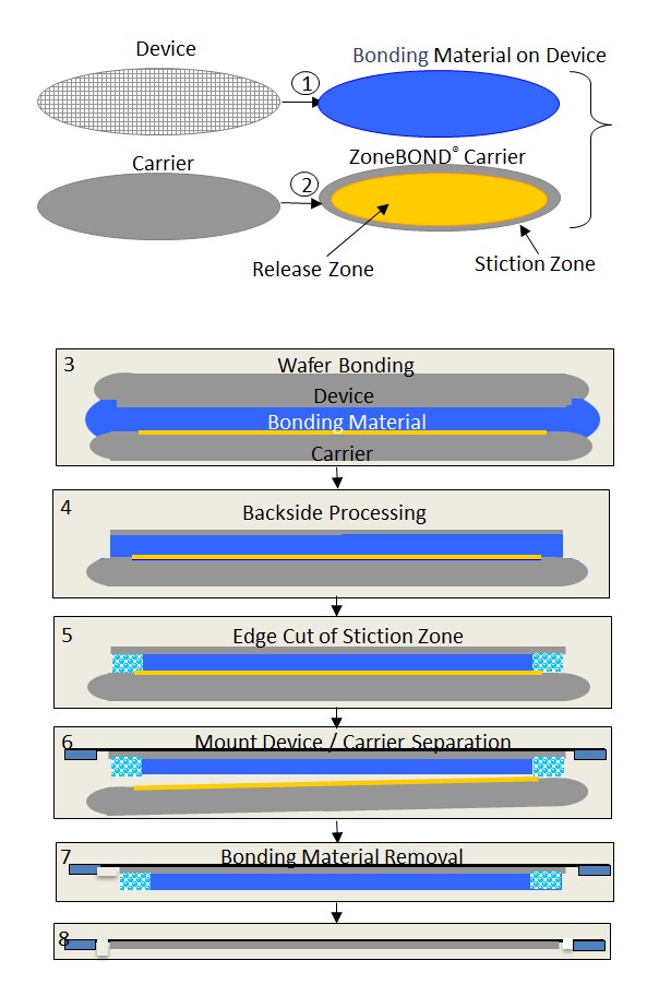
Smith of Brewer Science detailed the separation technologies available for their ZoneBond Process. The temporary adhesive ring of the ZoneBond process can be removed either by immersing the temp bonded wafer on a perforated carrier in a solvent bath as shown below:


Or,  by trimming the narrow bonded ring post fabrication to release the device wafer, where:
-          Debonding occurs at room temperature.
-          Separation occurs at the carrier-to-adhesive interface, not the adhesive-to-device interface.
-          Device is mounted in the film frame and is firmly supported on a vacuum chuck during debonding.
 This allows higher-temperature-capable adhesives
-          Thermally stable in bonded pair to 240°-260°C (depends on processing parameters)


Dow Corning
Ho of Dow Corning presented their new silicone based bi-layer temporary bonding solution. Their Bond/Debond Process Flow is shown below.
- Spin-coat bi-layer (release and adhesive layer)
- Room temperature bonding / debonding
- post-bonding cure on hot plate
- no plasma or lasers necessary
- fast mechanical debonding


Dow Chemical
Gallagher of Dow Chemical detailed their photo and laser patternable plating resists and dielectrics for WLP and 3D TSV.
Their Novolac (positive) and Acrylate (negative) resists are capable of a brad thickness range.


Their Cyclotene (BCB) dielectrics are laser patternable and their Intervia (epoxy) dielectrics show excellent vertical sidewalls. They also highlighted BCB as a temporary bonding solution which shows high thermal stability during backside processing ( , 1% weight loss at 300 C per hr) and clean RT mechanical peel-off debonding.   
Suss
Lutter, of Suss, compared the temporary bonding solutions that Suss supports focusing on the room temp mechanical debonding solutions.
 
 
The mechanical release at RT is described as follows:


Zonebond and several other solutions show excellent TTV (2-3um) after thinning to 50um.


Flex frame tape is a key to good debonding and cleaning . The principle of Suss debonding is shown below.


IEEE 3DIC
The IEEE’s premier 3DIC conference is on tap for the USA again this year. The conference will be held in San Francisco the first week of October. You can register here [link]
Lets take a look at the program:


 Wednesday, October 2nd  - Free Tutorials !
 13.00 – 14.00 Tutorials: 2.5/3DIC Players, Products & Markets, Rozalia Beica – Yole Developpement
14.00 – 15.00 Tutorials: 3DIC - Prof. Mitsu Koyanagi, Tohoku University
15.00 – 16.00 Tutorials: Design for 3DIC, Prof. Paul Franzon - NCSU
16.00 – 17.00 Tutorials: TSV and Interposer Design for High Performance and Low Noise,  Kim - Kaist
17.00 – 18.00 Tutorials: Monolithic 3DIC, Zvi Orbach
Thursday, October 3rd
08.30 – 09.45: Keynote Speaker: Prof. M. Taklo, SINTEF, Title:” E Brains”
09.45 – 10.15: Invited Talk I “ 3DIC Activity at Tohoku “  Prof. Mitsu Koyanagi, Tohoku University
13.00 – 13.30: Invited Talk II – “A Perspective on Manufacturing 2.5/3D”  Robert Patti, Tezzaron
17.00 – 18.00: Panel Session “Progress and Outlook for 3D ICs and 2.5D Systems -
Moderator: Jan Vardaman, TechSearch
Friday, October 4th
08.30 – 09.00: Invited talk III “The DARPA ICECool Program”  Avi BarCohen, DARPA
Hope to see you all there ….
For all the latest in 3DIC and advanced packaging stay linked to IFTLE…....