Monday, September 19, 2011

IFTLE 67 2011 Semicon Taiwan SiP Global Summit: 3D Technology part 1

The SiP global summit was held recently at 2011 Semicon Taiwan in Taipai. It consisted of the 3D IC Test Forum "Test Challenges and Solution in the New Era of Heterogeneous Integration" chaired by Mike Liang, President and CEO, KYEC; the 3D IC Technology Forum, "Embracing the Era of 2.5D & 3D ICs" chaired by Dr. Ho-Ming Tong, GM and chief R&D officer, ASE Group; and the Embedded Substrate forum, "Bridging the Last Mile of Heterogeneous Integration" chaired by Dr. Kuo-Ning Chiang, Professor, director, Advanced Packaging Research Center, NTHU.

Chairman Tong stood by the prediction he made at last year's meeting that serious commercialization of 2.5D and 3D ICs would likely begin in 2013.

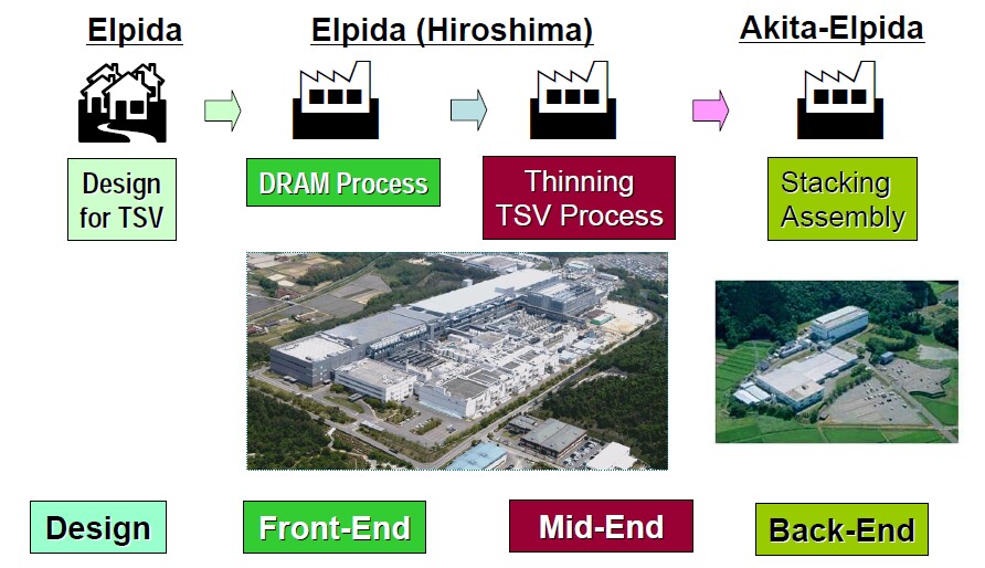
Takayuki Watanabe, VP of Elpida's TSV packaging development group, gave a detailed presentation entitled "TSV Technology for 3D DRAM." He described TSV production flow in Elpida where DRAM production and thinning is done in Hiroshima and stacking and assembly in Akita-Elpida.


Their memory stacking process flow is shown below:


In July Elpida announced sampling of their 8Gb DDR3 SDRAM [see "Elpida begins sampling 8Gb DDR3 SDRAM"]. The device is a "low power 8Gb DDR3 SDRAM that consists of four 2Gb DDR3 SDRAMs fitted to a single interface chip using TSV." Elpida believes that the new devices in notebook PCs will demonstrate a 20% reduction in operating power and a 50% reduction in standby power compared with systems that use the standard SO-DIMM configuration. Power consumption is reduced because the TSVs shorten the interconnect between the chips, thus reducing parasitic resistance and capacitance. In addition, chip height is decreased and the DIMM socket is eliminated. Chip mounting area is reportedly reduced 70%.

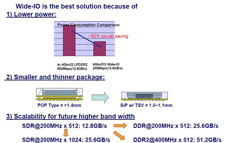
A 16Gb module (consisting of two 4 chip stacks) occupies far less room (11mm × 15mm) than its SODIMM equivalent (67mm × 30mm) Details of the power savings comparison are shown below.


Wide IO memory technology appears to be the future for mobile products mainly because it brings lower power consumption in a smaller, thinner package while being scalable for future bandwidth requirements. JEDEC is currently working to develop standards for such wide IO memory products.


About a year ago Elpida Memory, Powertech Technology (PTI), and United Microelectronics Corporation (UMC), announced a 3-way 3D IC partnership to Elpida had previously announced their partnership with Powertech Technology Inc. and UMC to build 3D chips for the mobile, high-end graphics and computer markets. [see IFTLE 8, "3D Infrastructure Announcements and Rumors"]

In terms of supply chain, Elpida/UMC/PTI propose the following:


In a separate presentation, Scott Jewler, chief engineering, sales & marketing officer for Powertech Technology, showed their prototype line and the state of construction of their high-volume manufacturing facility.

More info from Semicon Taiwan is coming soon. For all the latest in 3D IC and advanced packaging stay linked to IFTLE............................

Saturday, September 10, 2011

IFTLE 66 3M / IBM Seek to Improve Thermal Underfills; TSMC in Back End Packaging, Again

New thermal underfills for 3D chip stacking

Earlier this week 3M and IBM announced that the two companies "plan to jointly develop the first adhesives that can be used to package semiconductors into densely stacked silicon "towers" [...] which will make it possible to build [...] commercial microprocessors composed of layers of up to 100 separate chips." While giving little technical detail, they announced that this proposed program could "potentially leapfrog today’s current attempts at stacking chips vertically" and offer low power solutions for "makers of tablets and smart phones". IBM was quoted as saying that IBM scientists are "aiming to develop materials that will allow us to package tremendous amounts of computing power into a new form factor -- a silicon "skyscraper." The picture that came along with the press release is shown below. It certainly makes it look like the chips are actually being simply glued together, but if this is 3D stacking with TSV then this would be a chips-last solution, and certainly that cannot be done with more than two layers at a time. My assumption was that this was an oversimplification for the non-technical press release.

With the help of 3M and IBM I have made contact with Herve Gindre, division vice president at 3M Electronics Markets Materials Division, and Bernie Meyerson VP of research at IBM, to clarify exactly what is being proposed.

3M’s Gindre indicates that indeed what we are talking about is basically a thermally-enhanced underfill, which he says "will help conduct heat through 3D multichip stacks and/or away from heat-sensitive components circuits." 3M will staff the program in the semiconductor division of its Electronic Market Materials business, which currently provides temporary bonding solutions and CMP consumables to the 3D market place. Gindre points out that 3M will be focusing their "years of commercial experience in composites, nanotechnology, adhesives and thermal interface materials" on the current problem.

IBM will be running the program out of its semiconductor business unit. VP Meyerson declined to share much detail on timing or technology, which is to be expected since the program hasn’t even started. In terms of thermal performance specifications Meyerson offered that "we clearly wish to exceed current thermally conductive adhesive specifications to the point where the newly developed adhesive solutions at worst match those of silicon."

IFTLE will be following any further developments in this interesting program.

TSMC continues to scope out high-end IC packaging opportunities

Digitimes reports that TSMC has undertaken in-house high-end packaging of ICs, produced by its foundry processes, for fabless IC design houses in the US and Europe [link]. This would obviously create competition for Amkor, ASE, SPIL, STATs and other subcontractors.

At the last several TSMC spring Technology Symposia, in Silicon Valley, TSMC announced plans to expand its efforts in IC packaging. [see PFTLE 30, "Foundry TSV are comin’ -- TSMC makes their play for a biggerportion of the pie"] They have been doing wafer bumping, wafer sort, and wafer-level chip-scale packaging on a limited scale for years. At present, the company has two wafer bumping facilities, located in Hsinchu and Tainan. They are expanding their bumping and wafer-level chip-scale packaging technology and have announced copper pillar bump technology on 100μ bump pitch and will be manufacturing silicon interposers with TSV for 3D stacking. TSMC has announced that it is developing the interposers for Xilinx next-generation FPGAs and is in fact bumping them in-house rather than having that done at one of Taiwan's OSATS [see IFTLE 23, Xilinx 28nm Multidie PPGA…" and IFTLE 43, "IMAPS Device Pkging Highights: 3D IC"].

According to that Digitimes report, "fabless IC design houses are willing to have TSMC responsible for front-end foundry and back-end packaging services although TSMC's packaging ASPs are higher than those of IC packaging/testing service providers." They conclude that this is because these fabless IC design houses like the convenience of a one-stop solution and worry about lower yield rates due to outsourced packaging. However, their sources add that "interestingly, so far, no Taiwan-based IC design houses have accepted TSMC's higher quotes for packaging services."

Indications are that TSMC can generate gross margins of 50-60% for foundry services but even with their higher prices only 20-30% for packaging services. Thus some are questioning why they would expend precious equipment capex on the packaging side.

Whatever your take is on this new information, it is clear that TSMC is slowly but surely moving into what was before a clearly defined packaging and assembly space.

Update on Lester Lightbulb and the LED space

Several of you have tried to leave comments on IFTLE 63, "Bidding Adieu to Lester Lightbulb" and one of you was actually peeved enough that you couldn’t, that you contacted our editor Jim Montgomery. Thanks for that, because it exposed a flaw in the new software that appears to be blocking comments. Jim says they are working on it. One issue appears to be my reported price for the EnduraLED 60W equivalent. One reader claims he has found them for $39 and even $19. Jim got interested in this and tells me that he can now find them for both prices in different parts of the country. All I can tell you is that the Home Depot price on the day the blog was written was $47. The one that I now have installed actually cost me $49.99 since I bought it locally (and still have the receipt). Anyway, my point is not that the price would never come down, but rather how far down it had to come to make purchase of this device a good business decision vs the CFLs. Both bulbs are still glowing brightly -- as well they should, well past my lifetime expectancy if I am to take their marketing propaganda seriously.

Two other readers sent me email indicating that my concern over the life expectancy of the components in the bulb were well-placed, and that this certainly was not taken into account by Philips in their lifetime claims. I guess only Philips can answer that question.

For all the latest on 3D IC and advanced packaging stay linked to IFTLE……………………………………..

Saturday, September 3, 2011

IFTLE 65 Samsung’s 32GB RDIMM DDR3, GLOBALFOUNDRIES Packaging Alliance, Ziptronix Licensing News

Samsung Develops 30nm-class 32GB DDR3 for Next-generation Servers, Using TSV Technology

In December of 2010 IFTLE announced “the Era of 3D IC had arrived“ following the commercial announcement by Samsung that is was beginning the mass production of 8 GB DDR3 memory modules based on the SODIMM form factor [ see IFTLE 27, “The Era of 3D IC has Arrived with Samsung Commercial Announcement”].

Samsung has just announced the development of 32 GB DDR3 memory module (RDIMMs) using their 3D TSV packaging technology and their advanced 30 nm 4 Gb DDR3 chips. The modules can transmit at speeds of up to 1,333 Mbps, a 70 percent gain over preceding quad-rank 32GB RDIMMs (operational speeds of 800Mbps). Further, the 32GB-module consumes 4.5 watts of power per hour, reportedly the lowest power consumption level among memory modules in use in enterprise servers.
Samsung has issued engineering samples of its new modules and is currently collaborating with CPU and controller designers to expand support for 3D TSV server modules.

GLOBALFOUNDRIES and Amkor enter Alliance for Advanced Assembly and Test Solutions
GLOBALFOUNDRIES and Amkor have announced that they have entered into a strategic partnership to develop packaging solutions for advanced silicon nodes. Amkor is thus the founding member of GLOBALFOUNDRIES’ new “Global Alliance for Advanced Assembly Solutions”. GlobalFoundries indicates that they expect to strike similar deals with other companies to create a broader alliance of packaging partners.
As we have detailed many times in IFTLE, the move to advanced technology nodes has caused  packaging and interconnect solutions to become increasingly important. Packaging techniques are leading to improvements in performance and power-efficiency as well as reduced costs. IFTLE readers know that the adoption of 3D IC stacking of ICs is increasingly being viewed as an alternative to traditional technology node scaling at the transistor level. It is also clear that the ability to deliver end-to-end solutions such as 3D IC for customers will require such partnerships between foundries and OSATS to better enable supply chain management.

At their recent “Global Technology Conference” [link] Gregg Bartlett, Sr VP of technology and research and development at GLOBALFOUNDRIES noted that “..the market is beginning to crystallize around certain subsets where system designers want to have that [3D IC]capability in hand,  he continues that “…customers will be demanding 3-D chip stacks late in the 28-nm node or early in the 20-nm node… big graphics and networking chips will demand 3-D chip stacks using interposers…mobile apps processors will want 3-D stacks using through silicon vias”. But, he warned, "…the [3-D IC] supply chain is nearly as complex as the technical solutions".[link]
Indeed previous Globalfoundries roadmaps have shown 3D becoming “enabling” post the 32 nm generation.

Ziptronix signs licensing agreement with Sony
Ziptronix, Inc. has announced a licensing agreement with Sony Corporation for the use of Ziptronix’s patents regarding oxide bonding technology for backside illumination imaging sensors.
Ziptronix has been touting their Zibond™ oxide bonding technology for use in backside illumination (BSI) of CMOS image sensors for several years [ see  PFTLE 40, “Backside Illumination (BSI) Architecture next for NextGeneration CMOS Image Sensors]

 A back-illuminated structure minimizes the degradation of sensitivity to optical angle response, while also increasing the amount of light that enters each pixel due to the lack of obstacles such as metal wiring and transistors that have been moved to the reverse of the silicon substrate. Most of the CIS manufacturers have already moved to BIS technology per a recent market study by Yole
Developpment [ see "CMOS Image Sensors Technologies and MArkets - 2010". CMOS BSI sensors BSI sensor technology is being used by Sony and has been announced in video camcorders and digital still camera products by Casio, Nikon, Ricoh, Samsung, JVC and Fujifilm among others. Ziptronix CTO Paul Enquist asserts that their patented ZiBond™ technology, “…enables the industry’s lowest distortion for imaging systems utilizing backside illumination because of the oxide-oxide bond, alternate solutions, such as adhesives, fail to meet the industry need for ultra low distortion. ”


In December 2010 Ziptronix filed a complaint against TSMC and Omnivision in Federal Court alleging infringement of several Ziptronix low temperature oxide bonding patents [see IFTLE 31, " Oxide Bonding Patent Litigation Has Begun"] .
 With Sony taking a license on the Zibond technology can Samsung, Toshiba, Cannon, Panasonic, Aptina, ST Micro or others who practice BSI  be far behind ?
Ziptronix CEO Dan Donabedian predicts “… todays digital cell phone cameras that feature up to 5
Megapixel cameras can advance to 16 megapixels using Ziptronix’s patented technology” and similar impact will be seen in “…digital still cameras, digital video cameras, automotive sensors and projection systems such as pico projectors”.  Chris Sanders, Dir. of Business Development notes that Ziptronx is currently “…actively engaged with multiple companies across the globe for licensing our technology in the bsi image sensor space” 

For all the latest on 3D IC and advanced packaging stay linked to Insights from the Leading Edge………


Saturday, August 27, 2011

IFTLE 64 Semicon 2011 TechXSpots on “beyond 40 nm” and “3D deep sub micron”

The TechXSpot “Challenges and Solutions for 40nm and Beyond” was put together by Rich Rice of ASE and Tom Gregorich of Media Tek. Jim Walker of Gartner took a look at the macro trends effecting our industry including packaging.  Walker proposes the following :

- between the 45nm and 8nm nodes, logic fab costs will double to $10 billion.
- only four companies will be able to follow Moore’s law by 2018
- the annual number of new fabs built will fall by 60% between 2011 and 2015
- by 2015 foundries will account for ~ 1/3 of the value of all semiconductors compared with ~ ¼ today
- by 2012, over 50% of packaging/test (SATS) will be outsourced
- by 2015 more than $30 billion in annual R and D expense will be saved by collaborative R and D.

Gartners estimation of total capacity availability by node and year is shown below followed by the fact that the finer feature chips are the ones driving packaging advances. Walker pointed out that between 1980 and 2010 the number of different packages available on the market has increased from 30 to more than 2200 !


The TechXSpot session 3D in the deep submicron era was led by Jie Xue, Cisco Systems and Gamal Rafai-Ahmed, AMD .

Eric Beyne of IMEC addressed the integration challenges for 3D-TSV with advanced devices.
Beyne pointed out that the M1 metal layers “above” the TSV consist of very narrow, high aspect ratio lines which require very flat surfaces: low dishing of Cu TSV CMP. The ULK dielectric layers in lower metal layers are of reduced strength which requires stable mechanical properties in the TSV i..e quire optimized post-plating annealing conditions to avoid copper protrusion.

Semiconductor devices are very strain-sensitive. Strain is actively used to increase the mobility in the nMOS and pMOS FET channels. The stress induced by the Cu-TSVs may cause variability among devices. The use of higher stress in the device channels reduces the impact of small variations due to TSV’s.  The strain in the Si substrates will impact planar devices differently than FINFET devices which are somewhat “decoupled from the substrate”.
To reduce the impact of TSV stress on devices, a keep-outzone is defined around the TSV structure. For advanced nodes, reducing this KOZ to a minimum becomes more important.  The maximum stress induced in the Si by the TSV is in first order independent of the TSV diameter.  The stress levels in the Si are proportional to (ØTSV/r)2 , with r the distance to TSV center, thus scaling down the diameter of the TSV by x reduces the “effective TSV area” (TSV+KOZ) by x4 ! [As we have noted mnany times in IFTLE, the smaller the TSV (diameter and AR), the better]

Jon Greenwood of GlobalFoundries addressed backside integration and supply chain challenges.
When comparing 2.5 vs 3D integration Greenwood pointed out the following:
2.5D Integration
- For high performance applications, interposer option provides a thermal solution for near memory integration
- TSV technology is required to enable Si interposer
- Enables early TSV adoption
- Bridges design readiness, TSV impact and CPI concerns on device
- Typical interposer at 100 um thick allows time for back side and thin wafer handling processes to mature (increased system level yield)
3D Integration
- TSV middle technology is integrated into foundry process flows and node development
- Quickly becoming low power and mobile centric due to thermal management concerns
- Small form factor, high bandwidth applications
- TSV design and layout is critical to device performance and reliability
- Final device thickness typically at 50 um
- Additional yield concerns associated with thin wafer handling
They offer the following as what they view is becoming the standard TSV and backside processing flow.

In terms of supply chain they envision the foundry plus vs the OSAT plus vs the third party models as shown below where the manufacturing solution, reliability and warranty ownership is in the hands of the foundry, the OSAT or the 3rd party respectively. Its probably pertinent to insert at this point that the Xilinx program choose to have TSMC manufacture and FC the interposer and thus chose option #1.

Finally GF points out that while the substrate industry is stable and reliable, interposer delivery is a complete unknown.

GF concludes with the following thoughts:
 - An integrated supply chain that offers customers yield accountability and competitive pricing needs to emerge
- Interposer model needs to follow the organic BGA supply chain progression from the early
1990’s to today
- Japan Centric growing to Worldwide Supply Chain with multiple HVM suppliers located
throughout Asia
-Significant cost reduction and competitive pricing evolution –i.e.  over 90% cost reduction vs
today’s pricingspan>
- Substantial advancements in technology such as thickness reduction and warpage control, laser
vias, build up technology.
Ron Huemoeller of Amkor offered the following roadmap for silicon interposer products. While Amkor sees many TSV based products requiring an interposer, they see a severely constrained supply chain which is negatively impacting product proliferation.

For all the latest on 3D integration and advanced packaging stay linked to IFTLE…………………….


Sunday, August 21, 2011

IFTLE 63 Bidding Adieu to Lester Lightbulb

During the decade that my boys were growing up in Massachusetts, Massachusetts Electric had a great commercial on TV called “Lester Lightbulb” . Basically an incandescent light bulb with a smiley cartoon face on it told kids to remember to shut off the light when not in use and to not to put things into the electrical sockets. Energy savings is a good thing no matter what your politics are. Well I’m sure that most of you have heard that the US congress has convicted Lester of “wasting energy” and Lester is set to be executed next year unless someone can get him a clemency deal.

I decided to take a look at the case against Lester and while doing so look at the packaging that reportedly is being used for his preferred high tech replacement …the LED.
Everyone knows the acronym KISS – or keep it simple stupid. Certainly Lester the lightbulb which has been around for more than 100 years obeys that law. I guess thats why mass produced light bulbs cost < $0.50 each.

The US Energy Independence and Security Act of 2007 mandates new power consumption levels
for general service lamps by lamp wattage starting in 2012. Current  100W, 75W, 60W, and 40W incandescent products will be required to consume no more than 72W, 53W, 43W, and 29W, respectively. The DOE very carefully states that the “EISA does not ban incandescent lamps; it increases the minimum efficacy levels” but it is very clear that there will be no imports and no manufacturing of bulbs that do not meet these requirements [link].

There are an estimated 5B bulbs in use today. Anyone  wondering why the LED folks are going after the lighting market ?
Compact fluorescents have been fully commercial now for several years and also use significantly less power than our friend Lester. Like their tubular precursors, CFLs contain a small amount (typically five mg ) of mercury. Mercury is toxic and especially harmful to the brains of both fetuses and children. Its use in applications from thermometers to automotive and thermostat switches have been banned. When a bulb breaks the mercury can be inhaled from the air or can settle into the carpet for future slow release toxicity. In many locations it is already illegal to throw fluorescents out with regular garbage, however recent  recycling data ( Association of Lighting and Mercury Recyclers) estimates a residential mercury bulb recycling rate of a mere 2 percent. The current energy star (EPA rating) average lifetime for CFLs is listed as 8000 hrs. [link]
Popping open a CFL reveals a small PCB with ~ 20 components (mainly passives) loaded on its top surface. A bit more complicated than our old friend Lester.

The U.S. Department of Energy has had a competition running to find a viable replacement for the  60-watt incandescent . It was just announced that after 18 months of testing the Philips Lighting North America bulb had won the DOE’s $10MM prize. The bulbs had to meet or exceed these requirements: “greater than 900 lumens at 10W or less for an efficacy of greater than 90W/lm at a color-corrected temperature of 2700-3000K and a color rendering index of at least 90”. The Philips bulb reportedly exceeded all these requirements during the 18 month trial. Original requirements called for a target retail price of $22 for the first year, $15 for the second year, and $8 in the third year they were offered for sale. Philips has said it plans to offer the bulb for retail sale as soon as early 2012 although reports are that it will sell for ~$60 due to the higher cost of its materials content.

Philips already sells a 60-watt equivalent, the “EnduraLED” , at stores like The Home Depot,  although the prize winner is reportedly even more efficient. The prize bulb uses just 9.7 watts to match the light output of a 60-watt incandescent, compared with 12.5 watts for the product currently sold. The new lamp is also brighter than the one marketed now, at 910 lumens versus 800 lumens and reportedly  closer in color to a standard incandescent. The current EnduraLED (60-watt equivalent) currently sells for $47. The Warranty is 6 years, and Philips rates it at 25,000 hours of operation “it should last for decades if you take good care of it”. We’ll look more at the lifetime later in this blog.

I am pleased to report to you that the CEO of Philips Lighting North America, reports that “...the origins and development of this product, as well as its future manufacturing are all in the United States…. In addition, we have publicly said we will use the L Prize money to expand the manufacturing of this product in the United States. We will do this internally [at Philips facilities] as well as with American partners”[link]. To which I say BRAVO…..seriously BRAVO !.
In terms of  lifetime tests, “….200 bulbs were installed in a lumen maintenance test apparatus in which ambient temperature was maintained at 45°C to simulate the elevated temperatures common in enclosed lighting fixtures. The bulbs were operated continuously. Spectral measurements were taken on each bulb every 100 hrs for the first 3K hrs and every 168 hours (weekly) thereafter. Data for the first 7,000 hours of operation were used to predict lumen output of the bulbs at 25,000 hours. Lumen maintenance is predicted to be 99.3% at 25,000 hours, significantly exceeding the 70% L Prize requirement [link].
I personally would have an on off cycle where the bulb was switched off and then back on every 3 hours to mimic the daily use because we all know that bulbs usually burn out in the power on cycle, not while they are lit (at least that’s true for incandescants). This also only indicates to me what the projected light output would be at 25K hrs, not that the bulb will be functional after 25K hrs. More on that later.
I looked for a teardown of one of these bulbs to see how they were packaged and found one [link]

(A) The yellow plastic is the phosphor coating on the cover. Because it is located separately from the LEDs its called a remote phosphor. Popping off the phosphor coated covers we see the LEDs mounted vertically on the interior central column on the bulb. The LEDs are mounted on a little PC board which is a bit more complex than the CFL board (tongue in cheek) . The large amounts of metal (this is one heavy bulb) are used as the heat sink to conduct the heat away from the LEDs.
I decided to do just a little math to see if I could justify all the enthusiasm being generated for this bulb (after all the advertising on the Philips LED package says I’ll save me $147 over the life of the bulb !)
Below shows what I was able to find selling at my local Home Depot (An American hardware store).


The DOE tells me that “60W-equivalent LED A-lamps (the one listed in our table) at $40 per bulb is 6.3 years at average electricity rates.


The government officials like to point you to the “hypothetical” curve of the $5 LED bulb which pays off in 0.8 years , but…well if Lester had a voice he’d say that if a Mercedes cost $10,000 he would buy one of those instead of a Ford fusion….know what I mean.
My local Duke Power rate is 0.08/kWH and both I and the Govt agree that a light bulb is probably on for about 3 hrs a day. So the incandescent that lasts for 1000 hrs gives me 333 days of use or 0.91yrs and costs me : 3hrs x $0.08 /KWH x 0.06KWH/hr = 1.4 cents per day or $5.25/yr  or a bulb + power cost of $6.17 / yr . Using the same calculations CFLs would run $2.40 / yr and the LED would cost $2.16/yr.
Lets look at the Philips claim of $142 savings. Going out to 25,000 hrs (at 3 hrs/day thats 22.8 years ! - Hard to know what energy will cost 2 years from now let alone 23 years from now, but at todays prices the total cost for 23 years for the LED bulb is $49.68 vs our friend Lester at $141.9 for a net savings of $92 or a savings of $4.00 per year per bulb ( Philips must be counting on the price of power going up in their calculations).


Conclusions:
(1) The CFL and LED technologies, while they will certainly use less energy, are much more complex and simple volume scaling will not take them to the cost of an incandescent bulb.
(2) Are all the components on the PCBs really rated for 7.3 let alone 23 years use ? That’s longer than the ATandT telecom standards ! I am not convinced that anyone has determined whether all the passive components currently used on these devices will last that long and if they don’t, it will not matter if the bulb was outputting 800 lumens at the time that the bulb failed. As we all know, a device is only as good as its weakest component.
(3) Savings are tied to two main variables: (a) cost of power and (b) lifetime of weakest component. Increased price of energy makes them look better and failure of any of the components in the bulb will make their relative price increase significantly. For instance if a capacitor fails on the LED bulb after 4 years the new cost would be $12.80 / yr or double the cost of an incandescent. In fact the LED bulb needs to last 9 years to be equal to the cost of the incandescent.
(4) Since the CFLs will cost more than 7X less than the LEDs most families, when faced with changing > 20 bulbs per household in the period of a year, will move to CFLs. Changing 4B bulbs to CFLs in a year will increase the mercury released to the environment by ~ 20,000 Kg with much of this concentrated in the urban areas where our population is concentrated.
(5) IFTLE predicts that theft of light bulbs from public places will increase significantly in the future !
IFTLE has purchased said CFL and LED bulbs and they became operational on 8/15/2011. I will report back to you periodically on our real life testing. The breakeven point will be 8/15/2020 …….. anyone taking bets ?
For all the latest on 3D IC integration and advanced packaging stay linked to IFTLE……………

Monday, August 15, 2011

IFTLE 62 3D and Interposers – Nomenclature confusion; Equipment Market Shift to Pkging Continues

Some of you might remember a  late 1970s comic routine called "Raymond J. Johnson Jr" The character (shown at left) becomes annoyed when addressed as "Mr. Johnson" and exclaims  "My name is Raymond J. Johnson, Jr...now you can call me Ray, or you can call me J, or you can call me Johnny, or you can call me Sonny, or you can call me Junior; or you can call me Ray J, or you can call me RJ, or you can call me RJJ, or you can call me RJJ Jr but you don't hasta call me Mr. Johnson!"


Lots of equivalent names for the same person. Sometimes that happens in science and sometimes the exact opposite happens where lots of different things are all known by the same name - for instance 3D.

3D Confusion
At the recent Suss Workshop at Semicon West, I started of my 3D IC status lecture by pointing out the confusion occurring in the trade press about the term "3D." Below is a copy of the slide that I used. The culmination for me was the report released by the Taiwan trade development council July 5 with the catchy headline "TSMC may beat Intel to 3D chips." With a title like that this piece was widely picked up by the trade press and reprinted dozens of times on blogs and web pages by that evening. The example that I gave on the slide is EE Times (because it is the most prestigious of the lot) who appropriately referenced the original source (which may I say many others did not do) . In this haste to get material out to "the readership," no one appeared to have read the article to see that the original report was comparing apples to oranges or in this case TSMC 3D IC with TSV to Intel's announced finFET 3D IC transistor structures [ see IFTLE 50 "Words of Wisdom"]. I'm sure the trade development council authors, simply didn’t know the technical difference but the "copy cats," those who cut/paste and reprinted ...well they either also lacked the technical acumen to know the difference or simply didn't read it. EE Times corrected the story on July 11, curiously the same day the blog "SemiAccurate" lambasted them for their reporting [link]
When it comes to 3D be careful that you understand what you're reading about and don't always trust that the author has the knowledge or took the time to do the same. 


Silicon Interposers, 2.5 D or Silicon BGA
Looking back over the development of what is now commonly known as "silicon interposers" or "2.5D" as ASE's CTO Ho-Ming Tong has been calling them [see IFTLE 18, "The 3D IC Forum at 2010 Semicon Taiwan"] long time IFTLE (and PFTLE) readers are aware that I was not initially enamoured by silicon interposers due to my past experiences in "MCM-D" technology and was calling them silicon BGAs for awhile.[ see PFTLE 79, "Experience or Prejudice? Si Interposers Using TSV"] My views moderated with time as it became clear that there were strong drivers for Si interposers, this time around [ see PFTLE 109, "You Cannot Resist an Idea Whose Time has Come"]
The other day I decided to google "silicon ball grid array" and come up with a patent issued to old friend Dave Palmer, recently of Sandia. To be exact we are talking USP 6,052,287 filed in Dec of 1997 and issued in April of 2000 which gives it another 6 years of life. If you're in the business of making or using such interposers, you might want to give this patent a look !
Others point to the IBM patent  3,343,256 (1964) "Methods of Making Through connections in Semiconductor Wafers" and contest the validity of the Sandia patent. Only a legal battle will truly tell !
Cannon latest to enter packaging market.
With the number of players decreasing with each succeeding generation of scaling [ see PFTLE 121 "IC Consolidation, Node Scaling and 3D IC"] it is only logical that front end IC equipment vendors would be looking at the IC packaging market as an area into which they can expand.
In  April 2009 , PFTLE openly proposed that Applied appeared to be positioning to become  a "one stop shop" for those interested in 3D IC (see PFTLE, "Samsung 3D 'Roadmap' That Isn't").  In June of 2010 I added Novellus to that list as they announced a series of products aimed at the wafer level packaging and 3D IC with TSV markets [ see IFTLE 3   "....on Finding the Beef and Finally Addressing 3-D IC"]

The latest equipment supplier joining the group is Cannon who  made its first foray into the semiconductor back-end packaging equipment market with a lithography tool for through silicon via (TSV) and bumping.   Canon modified their  front-end tool series to accommodate the thicker resist films used by TSV and bump structures.  The system's projection lens optics expose 52 x 34 mm, compared with the 26 x 33 mm area exposed by front-end tools.

For all the latest on 3D IC and advanced packaging stay linked to IFTLE............

Sunday, August 7, 2011

IFTLE 61 Suss 3D Workshop at Semicon West

This week, lets take a look at some of the presentations from the Suss MicroTech workshop “3D Integration – Are We There Yet” which was held at Semicon West in July.  

Eric Beyne,  IMEC Scientific Director for 3D Technologies, addressed the technical issues of carrier systems for 3D TSV thinning and backside processing. Beyne points out that right now silicon carriers are favored over glass because the glass, while transparent which allows for laser based optical debonding techniques, must be CTE matched to silicon over a large temperature range; ground to tight TTV specification (high cost ?) and has a negative effect on plasma based post grinding backside processes due to its low thermal conductivity.
After alignment and temporary bonding Beyne recommends the use of use of in-line metrology to allow for wafer rework if necessary.

Rama Puligadda, Mgr. for Adv. Materials R&D for Brewer Science gave an update on their ZonebondTM  room temperature debonding process.  The Zonebond process basically uses a 2.5 mm ring of adhesive to hold the wafer in place for grinding and backside processing which allows for easier subsequent debonding. The thin wafers are released from the carrier at room temperature after mounting on a film frame. Blanket UV exposure on the flex frame allows solvent removal of the temporary adhesive without damaging the adhesion to the flex frame tape.

Brewer has also developed a process with two carriers in order to achieve a wafer flip.


Stephen Pateras, Product Marketing Dir. at Mentor Graphics, gave a presentation on advanced design for test (DFT) and built in self test (BIST) for 3D-IC structures.  Pateras points out that TSVs can be used to create test access paths so that all BIST resources can be accessed on any device.

Pateras also concluded that all EDA players need to support common test access infrastructures since this will be required to stack die from difference sources. 
Eric Strid, CTO of  Csacade Microtech, indicated that they are using MEMS techniques to produce lithographically printed probe cards capable of 6 µm sq. x 20 µm high probe tips on 40 µm pitch which are being sold in research quantities.

Strid pointed out that standard pad locations will be required for vendor interchangeability and that standard materials specs for pads are needed in terms of materials, thickness and flatness. Such standard pad locations will enable standard test tooling.
Stefan Lutter , Bonder Project Mgr for Suss, discussed equipment and processes for temporary de-bonding. Suss reports that their open platform approach is capable of using any of the following bond/debond technologies. They see the industry trend as moving to the newer room temperature (RT)  release processes.


They claim that their HVM equipment, available 4Q 2011, will be capable of bonding and debonding 20-25 wafers/hr. The new Suss MicroTec product introduction is a HVM debonder/cleaner line for the RT release processes.
Thinned wafer on carrier mounted to flex frame are fed to these modules and thinned wafer on flex frame and detached carrier are generated. The technology uses a porous vacuum chuck to hold the thin device wafer that is mounted on tape and a flexible plate with vacuum grooves and debond initiator to peel-off the carrier. A schematic of the cleaning process is shown below.

For all the latest on 3D IC and advanced packaging stay linked to IFTLE