Anyway, the IMAPS Device Packaging Proceedings
have still not arrived (since March!), ditto on the April ICEP proceedings, and
the ECTC is yet a week away. So, I thought we might take “a
hot air balloon look” at our industry.
The
front end drives everything
Even though you came to this blog to read about packaging, clearly understand that packaging is driven by IC fabrication (the front-end) and that will never change.
IC fabricators make their big profits on the leading edge node, not on the older, more available nodes.
New materials are introduced on the leading edge, and once these processes are locked down (qualified), they are very hard to change. This is why equipment suppliers and materials vendors have always spent much of their hard-earned profits on trying to get qualified into the next generation node products.
The
End is Coming! Soon. Maybe.
Everyone reading this blog understands the “Moore's Law Coming to an End” arguments. Exactly when it will happen is, to me, less relevant than the fact that it is happening or has already happened for many mid-tier IC fabricators.
Some top-tier fabs / foundries will find a
way to move forward past 22nm to 14nm and beyond, but the important point is
that the vast majority won’t. This is not because the technology won’t be
available to them, but rather because it will be too expensive. You have seen my slides on this before. Since
it is very important that you understand it, I will show them to you again.
The conclusions are simple:
1. There are only a few companies with enough
revenue to justify developing and building $6B+ fabs for 22nm and beyond.
2. There are very few products that have
enough volume to absorb the design costs inherent to 22nm and beyond designs.
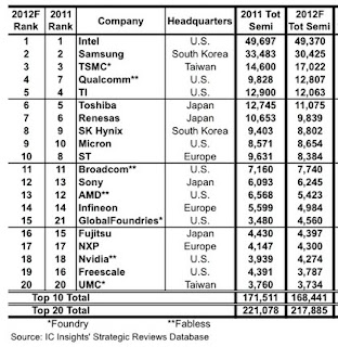
The players that can afford to move forward at
this point appear to be Intel, Samsung, TSMC,
GlobalFoundries, UMC and Hynix. Maybe one or two more appear through
consolidation, but, in general, that’s it.
Packaging
Is Becoming More and More Important…and valuable
In the future, product differentiation in most product lines will be achieved
by the packaging used, not by the incorporation of chips of the latest node. What we are seeing in the industry is TSMC,
Samsung and maybe others making a strong move into IC packaging.
Equipment
Vendors Consolidating as Customer Base Shrinks
For equipment vendors, the leading edge node customer
base is shrinking, and thus you see some of them (litho, 450mm) requiring
investments from the IC fabricators before putting money into future node
developments.
Typical front-end equipment vendors led by Applied
Materials, Lam etc. are also acquiring back-end equipment vendors to expand their
product offerings.
Front-end equipment vendor acquisitions in
back-end packaging equipment was, at
first, met with skepticism by the packaging community, since front-end equipment has
significantly higher margins than back-end packaging can afford. More recently,
they have realized that the front-end chip fabricators are moving into the back-end packaging business and are going to their traditional equipment vendors to
meet their needs.
Material
Suppliers Consolidation Coming ?
It is only logical that the next round of
consolidation will come from the materials suppliers.
Materials suppliers have traditionally been
quite ignorant when it comes to the actual applications where their materials are
to be used. Most blindly follow the roadmaps put out by the industry without
really understanding them. In several instances, the low K fiasco of the late
1990s comes to mind. They followed the Pied Piper right over the cliff with
many of them loosing tens of millions of dollars, trying to develop spin on polymer
dielectrics that were really never going to be used.
Materials suppliers, once again, need to be
very careful when developing for the sub 22nm nodes (on chip or packaging) or
for 450mm processes, because the number of companies working on these programs
is likely to be significantly greater that the number of potential customers. History
tells us that there will only be one or two processes / materials sets chosen
by these six-ish players and the potential losses incurred here, by the materials
suppliers whose solutions are not chosen, may in fact lead to the eventual consolidations
that I predict.
In addition, speaking to many fabs and
foundries they all appear to be attempting to minimize the number of suppliers they
engage as a cost containment issue. I will not be surprised to see old
qualified processes trying to replace generic materials with favored vendor
equivalents.
These are not unusual outcomes; in fact, they
are natural for an industry that is entering its “mature” stage, and that is certainly
where we are headed.
Hope to see many of you all in Vegas at
ECTC.
For all the latest in 3DIC and advanced
packaging, stay liked to IFTLE.


No comments:
Post a Comment