Continuing with key developments at the 2011 RTI ASIP
ST Ericsson / CEA Leti / CadenceOne of the best received presentations of the conference was “A Three-Layers 3D-IC Stack including Wide IO and a 3D NoC - a Practical Design Perspective –“ by Pascal Vivet, and Vincent Guérin. Going well past their allotted time during the scheduled presentation, they were brought back ( by yours truly) after the session ended to answer questions for a further 45 minutes. While some of the presentation was beyond the capability of the management and process development audience, the importance of the contribution was crystal clear to everyone.
“Wioming” is the first application processor SOC integrated with a Wide I/O memory interface which should enable superior graphics and CPU performance in smartphones and tablets. It is a high speed CMOS, TSV middle process with:
- multicore CPU backbone
- 4 wide IO memory controllers. Belived to be the first implementation of the JEDEC wide IO standard.
- 3D asynchronous network on chip (NoC) for logic on logic stacking
Scheduled for build are:
- Uses ST-Microelectronics high-speed CMOS library
- Uses TSV middle (10μm) + Copper Pillar (10μm) - Flip-Chip packaging assembly - Face2Back, Die to Die 3D stacking assembly - uses Cadence “Encounter 3D-IC” design implementation
Was taped out in fall 2011 and is currently in fabrication.
There is reportedly a ST Ericsson wide IO application processor product in planning that will use TSV technology.
IBM
Dan Berger IBM Manager of “3Di” development reiterated a concept that we have heard before from IBM namely that “You need a bullet proof TSV formation process to make this all work” and that right now the “Supply chain is the toughest nut to crack – It’s good to be an IDM”. IBM is currently using 45 nm CMOS and 130 nm SiGe chip processes on a 2.5D interposer with 90 nm wiring for their Semtech products, announced last fall [ see IFTLE 27,“Era of 3D IC Has Arrived with Samsung Commercial Announcement”] which are produced in Fishkill and their recently announced involvement with
Micron on their memory cube commercialization [ see IFTLE 74, “The Micron Memory Cube Consortium” ].
Yole Developpment
Yole’s Perkins commenting on the TSMC statement pointed out that there’s lots of money in play here, and other people ( OSATS) aren’t going to just walk away, but are going to look for alternative solutions. The now annual Yole 3D timeline is updated below.
STATSChipPAC [SCP]
Raj Pendse, VP and CMO for SCP gave an in depth presentation on their thoughts and approach to advanced packaging and 2.5/3D.
Sematech’s Arkalgud detailed the work at the Sematech “3D Enablement center” where the primary focus is on Wide IO DRAM for mobile and high performance applications.
Their goal is to “..provide clarity and help identify gaps in standards, specifications and technologies” Arkalud also indicated that Sematech is looking at next generation work on low time/temp Cu-Cu bonding technology that they are not at liberty to fully disclose yet.
Without providing specifics, one of the conclusions from their Sematech cost analysis is that “3D interconnect can lower the overall cost of ICs”
ASE
Hwang of ASE showed excellent electrical performance data for Cu bonded structures.
Qualcomm
Ray of Qualcomm said that they have determined that form factor and performance are the most critical elements for them and that the smallest form factor comes from 3D stacking so they would most likely go directly to 3D stacking.
Synopsys
Michael Jackson of Synopsis presented the following slide to rationalize why 2.5D is happening before full 3D stacking.
EVG
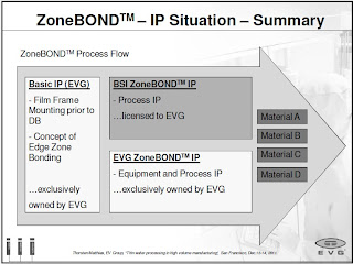
Mathias of EVG updated their status on the Zonebond™ process . We have discussed the technical details of Zonebond previously [ see “Is 3D Packaging Where it Needsto Be?” ] The EVG position is that:
EVG has worldwide access to Brewer Science ZoneBONDTM technology, including:
- The right to sublicense to any EVG equipment customers.
- The right to produce carrier wafers and EVG equipment customers to do so.
EVG owns own IP related to the ZoneBONDTM process and to ZoneBONDTM equipment and as shown below the right to use any materials for the process including .
- thermal release materials
- UV/IR release materials
- designated solvent release materials - thermal release materials
- UV/IR release materials
- designated solvent release materials
For all the latest on 3DIC and advanced packaging stay linked to IFTLE…………………..


No comments:
Post a Comment