Tuesday, November 8, 2011

IFTLE 74 The Micron Memory Cube consortium

Most of you by now have seen the announcement that Micron has joined with Samsung to create the "Hybrid Memory Cube (HMC) Consortium" with fellow founding members Altera, Open Silicon, and Xilinx. [link 1, link 2]

The consortium is built around Micron's hybrid (previously referred to as "hyper") memory cube technology. The initial goal of the consortium is to define specifications for HMC. The HMC interface is totally different, having nothing in common with current DDR implementations, so it is felt that standardization and adoption by major producers and users is the only way that HMC will become a standard memory product for the industry.

We have previously addressed the fact that the memory bandwidth required by high-performance computers and next-generation networking equipment has increased beyond what conventional memory architectures can provide. The term "memory wall" has been used to describe the problem. A solution to the memory wall problem requires an architecture that can deliver increased density and bandwidth at significantly reduced power consumption.

Micron initially announced their memory breakthrough earlier this year [see IFTLE 38: "Of Memory Cubes and Ivy Bridges -- More 3D and TSV"], and began releasing information at conferences this summer [see J.T. Pawlowski, "Hybrid Memory Cube: Breakthrough DRAM performance with a fundamentally re-architected DRAM subsystem", Proc. 23rd Hot Chips Symposium, 2011].

While DDR DRAMs have gotten bigger through the years by increasing the parallel arrays of DRAM cells on chip, they remain limited to the bandwidth supported by package I/O. DDR3-1333 and DDR3-1600 devices currently offer bandwidths of 10.66 Gbps and 12.8 Gbps respectfully. The HMC is a stack of multiple memory die sitting atop a logic controller chip bonded together using TSV. This greatly increases available DRAM bandwidth by leveraging the large number of I/O pins available through TSVs. Both the number of contacts and their shorter lengths enable dramatically higher data transfer rates than today's memory other memory architectures -- Micron has shown prototypes rated at 128 Gbps.

Current DRAM burns a huge amount of the power in laptops and phones. Brian M. Shirley, VP of DRAM solutions at Micron, claims that the company's hybrid memory cube technology "offers a 20-fold performance increase while reducing the size of the chip and consuming about one-tenth of the power," while occupying 10% of the volume of a DDR3 memory module.


[Performance & Power consumption Paradigm shift due to HMC (left); TSV stacked memory layers on logic layer (right). Source: Micron]


Micron reports that the HMC module achieves and exceeds 128 Gbps by using parallel channels. An image of the first-generation Micron HMC memory die showing the large number of I/O coming off each die:


[HMC Memory Device showing large Number of I/O. Source: Steve Liebson, Cadence EDA360 Insider blog]


Joe Jeddeloh, whose Micron team developed the logic portion of the HMC has described [link] the key "themes" of their technology as follows: "Instead of a DRAM die being one large device that has one set of I/Os on it, we break it into, say, 16 separate DRAMs, in essence much like a multicore processor. Each of those DRAMs has its own interface so when you go to access data, you go to a very local area of DRAM [...]It's a more directed access." Then, "we move that down the Z direction on a TSV."

When asked about the impact of 3D stacking on memory performance, Jeddeloh responded:
"When you think of a DIMM, maybe it has 4, 8, 16 [memory cell] banks in it, ...once you go to a memory cube where you have these tiles and partitions, each of those has its own bank structure. So instead of 8 banks, you have 128 banks, 256 banks and each of these are put into parallel DRAM structures so you have a tremendous amount of concurrency available. You can think of a many-core processor coming at a many tiled memory system that marries up and can handle a lot of concurrent transactions."


In terms of mating this memory to today's and future microprocessors, Jeddeloh commented that "As we go to more and more cores on processors [they become] more and more bandwidth-hungry. In this generation, you can't stack the DRAM on top of the processor because the processor is too hot. That means the processor has to go off-chip to get that bandwidth [and] you need to connect a pipe to that processor that can bring in as much bandwidth at the lowest amount of power." Micron's HMC technology, he explained, "can put more density in a very local area and put that right next to the processor." He also characterized power as the No. 1 theme going forward: "Once we reduce that power, we can create a smaller, more efficient I/O structure when the processor and the memory system are right next to each other. If you have, say, eight cubes hooked up to a processor, there's a tremendous amount of bandwidth and concurrency that can happen in a very small area."


Concerning heat issues in the HMC, Jeddeloh noted that "DRAM doesn't like heat; it messes up the refresh. If we are not on top of the processor, the heat is manageable. Once you create that low-power I/O [...] and you're not creating as much power within the cube itself, then you stack it up and pull the heat out the top."


[160 Gbps = 1 HMC or 15 DDR3-1333 DIMMS. Source: Micron Technology]


Scott Graham, general manager for Micron's Hybrid Memory Cube (HMC), predicts that HMC impact will be seen in multiple markets such as high-performance computing, networking, video, medical, energy, wireless communications, transportation, security -- basically any applications that will require the transfer of tremendous amounts of data. When asked about the Samsung partnership, he answered: "We need multiple sources for a broad adoption," since the industry is not comfortable with any sole source products. He indicated that the plan of record is to begin production in the second half of 2013.

At the recent Intel designer forum (IDF 2011) we found out that Micron teamed up with Intel to create the technology [link]. The company highlighted that a big impediment to scaling the performance of servers and data centers is the available bandwidth to memory:
"As the number of cores on a microprocessor increases, the need to feed the cores with more memory data expands proportionally. There [are] severe limitations to achieving high-speed and low-power using commodity DRAM [...] We came to the conclusion that mating DRAM and a logic process based I/O buffer using 3D stacking could be the way to solve the dilemma. We found out that once we placed a multi-layer DRAM stack on top of a logic layer, we could solve another memory problem which limits the ability to efficiently transfer data from the DRAM memory cells to the corresponding I/O circuits."


Intel CTO Justin Rattner demonstrated the Hybrid Memory Cube toward the end of his keynote lecture which can be seen here [link]. Rattner noted that the HMC was "the world's highest-bandwidth DRAM device with sustained transfer rates of 1 terabit per second (trillion bits per second). It is also the most energy efficient DRAM ever built."

It is currently unclear whether Intel holds any of this HMC IP -- and it is equally unclear why Intel was not a founding member of the HMC consortium. IFTLE will follow this evolving story closely.

For all the latest in 3D IC and advanced packaging stay linked to IFTLE..........

Saturday, October 29, 2011

IFTLE 73: Xilinx shows 2.5D Virtex 7 at IMAPS 2011

Xilinx 2.5D FPGAs

Liam Madden, corporate VP of Xilinx, gave the keynote presentation to kick off the 2011 IMAPS 44th Int. Symp. on Microelectronics a few weeks ago in Long Beach CA.
Last fall Xilinx announced a single layer, multi chip silicon interposer for its 28nm 7 series FPGAs. Looking at module assembly, first the four 28nm chiplets are mounted on a 25 × 31 mm , 100μm thick, silicon interposer with 45μm pitch microbumps and 10μm TSV. The interposer is then assembled on a 35 × 35mm BGA with 180μm pitch C4 bumps. The FPGA slices are connected by ~10,000 connections created on the silicon interposer. Compared to connections on a PWB, the interposer interconnect technology provides over 100× the die-to-die connectivity bandwidth per watt, at one-fifth the latency.


Madden indicated that the use of an interposer (known as 2.5D) was the right choice for FPGAs since the "10,000 routing connections" if they would have been TSV in the FPGA slices, would have used up valuable chip area making the chips larger and more costly than they are now.

TSMC is fabricating the chip and the interposer and bumping the interposer, while Amkor is bumping the chip and doing the module assembly. Madden gladly showed one of the modules to the packed audience:


[Madden showing Virtex 7 module with James Lu ( RPI) and GS Kim (CEO of EPworks) looking on]


Madden indicated that the Virtex 7 HT will consist of 3 FPGA slices and two 28gbps SerDes chips on an interposer capable of operating at 2.8Tb/sec. In their paper "Advanced Thermal study of Very High Power TSV Interposer and Interconnects for 28nm Technology FPGA," Xilinx details the thermal study of TSV interposer technology for high performance 28nm logic die mounted on a silicon interposer with Cu-filled TSV. Based on DOE experimental results optimized TIM material, underfill, bump pitch and passive heat sinks were selected resulting in the following optimized thermal results at 55°C or 75°C ambient. Simulation results confirm that for the selected passive heat sink the high power FPGA package is thermally reliable and meets thermal specs.


Xilinx also reported on quality and reliability in their paper "Quality and Reliability of 3D Interposer and Fine Pitch Solder Micro-bumps for 28nm Technology." Microbump (FPGA to interposer) resistance was measured from Kelvin structure measurements.


Interposer stress and delamination risk were carefully studied through simulation and thermal cycling. Simulation results indicated that the overall stresses in the silicon, SiO2 insulator and copper via are below the fracture strength of the given materials.

During package level reliability testing, the 3 main factors evaluated were type of underfill, top die thickness and interposer cleaning . Test samples were exposed to level 5 preconditioning, HTOL (high temp operating life) and TC (temp cycling). Reliability results showed that higher Tg underfills passed all tests . Failures were observed with lower Tg underfills. In addition proper interposer cleaning and die thickness reduction were necessary to prevent delamination.

Wafer applied underfills for 3D

IMEC addressed the "Use of Wafer Applied Underfill for 3D Stacking." In the case of die-to-package UF one is looking to mitigate the CYE differences between the laminate package substrate, the ~100μm solder bumps, the silicon die, and the package overmolding -- whereas in the case of die to die assembly such as 3D structures the underfill has to mitigate the CTE differences between the 2 silicon die and the ~ 10μm microbumps. Thus there are different requirements for the two.

In 3D packaging the main challenges for underfill are the narrow gaps between the chips and/or the chip and the substrate (~10μm) and the fine pitch between the bumps (i.e. 20μm). The use of capillary underfill (CUF) is time-consuming as requires excess space around the die for the dispense action. In the case of no flow underfill (NUF) the materials is dispensed on the substrate before the die stacking. Materials need to be transparent so you can see the alignment marks during the flip chip operation, dispense timing since this is still done for each individual die and underfill/filler entrapment between the bump and the pad.
For 3D, CUF is not an option due to the narrow gap and the fine bump pitch. NUF is a better choice but suffers from the transparency requirement and dispense volume control (i.e. excess underfill can be thicker than the bumps and thus hinder chip to chip bonding and/or squeezing out excess underfill can "backside overflow" (see pic below) which can contaminate backside pads.


Wafer applied underfill is considered a strong candidate for 3D because theoretically it can significantly increase throughput. It can be done by either spin coating or dry film lamination.


IMEC challenged 9 global underfill suppliers with the following criteria:

- Uniform material thickness ( < 30μm, target 10μm)
- Gap fill for <40μm bump pitch
- Transparent to allow alignment
- Tacky at ambient temp
- Low cure temp, usable up to 250°C

One spin coat and two dry film materials were submitted for testing. After initial testing IMEC was left with one spin on material and two dry films.


After fabrication of test vehicles IMEC daisy chain yields of 0% eliminated the "hybrid dry film" and resulted in 20%-50% yields for the remaining epoxy spin on and dry film. The latter two materials are being considered for further development.

3D activity at ITRI

John Lau and co-workers from ITRI gave several presentations on the various aspects of 3D IC that they are working on at ITRI, many of them tied to their 3DIC test vehicle. [ see IFTLE 52, "3D and Adv Pkging at ICEP 2011"]


In their paper "Oxide Liner, Barrier and Seed Layers and Cu Plating of Blind TSVs on 300 mm Wafers for 3D IC Integration" they focused on their process development for TSV filling. They use an AMAT PECVD to deposit TEOS SiO2. At 180°C deposition temperature they find that step coverage is improved by higher temp, higher Rf power, lower pressure, and lower TEOS flow.

For barrier layer and seed, a AMAT self ionized plasma PVD system is used for Ta barrier and Cu seed. They achieved < 50 pA leakage current between 10μm × 60μm TSV. In their paper "Thin Wafer Handling of 300mm Wafers for 3D IC Integration" IRTI points out that if your dicing tape adhesive strength is "too strong" it may strip immersion gold off of the chip pads. In their presentation "Wafer bumping and Characterization of Fine Pitch Lead Free Solder Micro bumps on 300mm wafers for 3DIC integration" they offer that the difference in volume between FC solder balls and micro bumps is > 20× and the smaller and thus IMC and Kirkendall void formation issues are more pronounced for the smaller bumps. For this reason ITRI does not reflow the micro bumps before joining and the micro bump assembly is usually fluxless to reduce the chance of entrapping flux during solder reflow. Underfills are more critical for micro bumps. UBM thickness is > 10× less and the budget for undercutting the micro bumps is much smaller meaning that the process windows are smaller.

For all the latest on 3D IC and advanced packaging stay linked to IFTLE..........


We have previously reported that the IEEE International 3DIC Conference was moved from its initial October 2011 date outside Tokyo to Jan 31st 2012 in Osaka due to the unfortunate earthquake/tsunami events of this past year. The US program committee, which was scheduled to hold the 2012 even in San Francisco in October 2012, has decided to postpone their event till 2013 in deference to the unusual events surrounding the 2011 Japan meeting. We strongly recommend support of the coming meeting in Osaka.

Sunday, October 23, 2011

IFTLE 72: 2011 IEEE 3D test workshop

For the second year the IEEE 3D Test workshop was held in conjunction with ITC (IEEE International Test Conference), with Yervant Zorian of Synopsys as general chair and Erik Jan Marinissen of IMEC as program chair. More than 125 attendees attended 11 sessions which covered all of the mainline test issues: Executive views (Synopsys, ASE, Samsung, Teradyne,Cascade, Cadence ect.); 3D electronic Design Automation (EDA); wafer probing; standardization; and challenges and solutions for wide IO DRAM stacking.

Unlike a few years ago where Universities were the main groups involved with developing 3D test protocols, the 3D Test workshop list of corporate sponsors now says all we need to say about the desire for the world's major design and test houses being involved.


Eric Strid of Cascade Microtech looked at the status of probing:


Brandon Noia and Krishnendu Chakrabarty of Duke University looked at "Methodology for Pre-bond Test of TSVs and Breakpoints in High Performance 3D-SICs." If we assume the following is the accepted 3D Manufacturing/Test flow:


The goal is to detect TSV defects prior to bonding (pre-bond) but we are faced with:
-- Pre-bond TSVs are single ended
-- Current probe technology: Minimum pitch 35μm but TSVs will be ≤5μm with pitch of ≤10μm and densities of ≥10,000/mm2


TSV test can be done by BIST (built-in self test) and DfT (design for test).


In a joint presentation between Cadence, IMEC and TSMC entitled Automation of DfT Insertion and Interconnect Test Generation for 3D Stacked ICs", Sergej Deutsch of Cadence concluded:
  • 3D test challenges include pre-bond and post-bond testing
  • 3D-DfT architecture
    -- I/O wrap and test-only pads for pre-bond testing
    -- Serial and parallel test access mechanisms
    -- Test turns: to bypass upper dies in stack
    -- Test elevator mode: for test paths to/from upper dies
    -- DRAM top control interface
  • 3D wrapper insertion flow
    -- Inserts 1500-style wrappers and 1149.1 for bottom die
    -- Includes controls for I/O wrap and DRAM testing
    -- Generates input to run ATPG
  • Industrial case study concludes: negligible area costs of 3D wrapper

Etienne Racine of Mentor Graphics gave a look at TSMC's RF12 reference flow for die stacked on interposer.


For wide IO DRAM they offer the following:


Larry Smith from SEMATECH's Standards group discussed the 3D Enablement Center, which was announced December 2010 by SEMATECH, SIA, and SRC. It is designed to meet SIA member needs in high performance, mobile, analog, mixed signal, MEMS, fabless, fablite, IDMs. Their mission: "Enable industry-wide ecosystem readiness for cost effective TSV-based 3D stacked IC solutions." Members include: ASE, Altera, ADI, LSI, NIST, ON Semi, Qualcomm, Hynix, CNSE, GlobalFoundries, Hewlett Packard, IBM, Intel, Samsung, TSMC, and UMC. Initial focus is on wide IO DRAM for mobile and high-performance applications:


Erik Jan Marinissen of IMEC updated the group on the status of IEEE P1838 the “3D-Test Standardization Study Group” chartered with defining the standards in 3D test and DfT. Their current project is P1838: “Standard for Test Access Architecture for Three-Dimensional Stacked Integrated Circuits”.

Focus:
-- Generic test access to and between dies in a multi-die stack
-- Prime focus on stacks with TSV-based interconnects

Test:
-- Pre-bond, mid-bond (partial stack), post-bond (complete stack)
-- Intra-die circuitry and inter-die interconnects
-- Pre-packaging, post-packaging, board-level situations

Die-centric standard:
-- Die-level features comprise a stack-level architecture
-- Compliance to standard pertains to a die (not to the stack)
-- Enables interoperability between die and stack maker(s)
-- Standard does not address stack/product-level challenges/solutions (e.g. boundary scan for board-level interconnect testing)
-- However, standard should not prohibit application thereof

Two standardized components:
-- 3D test wrapper hardware per die
-- Description + description language

Scan-based:
-- Based on and works with digital scan-based test access

Leverage existing DfT wherever applicable/appropriate:
-- Test access ports (such as IEEE 1149.x)
-- On-die design-for-test (such as IEEE 1500)
-- On-die design-for-debug (such as IEEE P1687)

Standard does not mandate:
-- Specific defect or fault models
-- Test generation methods
-- Die-internal design-for-test

Further info can be obtained here: 3D-Test WG or here: Project P1838.


For all the latest on 3D IC integration and advanced packaging stay linked to IFTLE..........

Monday, October 17, 2011

IFTLE 71: 450mm announcements

Moving to 450mm has several advantages, the main being that the area is 2.25× larger. This obviously means that more chips can be cut from one wafer, and less material is lost at the edges. The last conversion process from 200mm to 300mm wafers began in 2000, creating price reductions of around 30%-40% per unit. The elite of the global semiconductor industry now plan to move to 450mm wafers where a cost gain of 25%-30% is hoped to be achieved.

Although the initial goals from the triumvirate of Intel/Samsung and TSMC called for a 450mm pilot line to be ready in 2012 [link], it does look like things are finally getting off the ground.

Intel, GlobalFoundries, IBM, TSMC, Samsung create 450mm initiative

New York State has entered into agreements for $4.4 billion in investments over the next 5 years from Intel, IBM, GlobalFoundries, TSMC, and Samsung to create a 450mm consortium and manufacturing center there. Reportedly this will create close to 7000 jobs, 2500 of which would be high-tech. (Hopefully these reported job numbers are more realistic than what have been reported recently for "green jobs" and jobs created from the "stimulus.")

The facilities will be located in CNSE (College for Nanoscale and Science Engineering) "Albany NanoTech," CNSE's Smart System Technology & Commercialization Center in Canandaigua, SUNY-Utica, and IBM sites in East Fishkill and Yorktown Heights. New York State will invest $400 million in CNSE in Albany over a 5-year period.

The joint 450mm project will focus on transforming existing 300mm technology into the new 450mm technology. These technology developments "may facilitate the possibility of building a 450mm production line in New York state."

SEMATECH

Since 2006, the SEMATECH ISMI organization has been looking at the early stages of the 450mm transition, including developing standards for the wafers, automation, and getting agreement on the development of the 450mm processing tools. Last year, the entire ISMI organization moved to Albany, from Austin, and the state of New York invested an estimated $300 million in the 450mm program at ISMI. Intel headed up the ISMI 450mm program, and has been on point for many of the negotiations with the tool suppliers.

The announcement of the Global 450 Consortium consolidates the 450mm effort into one consortium, with access to the new CNSE Fab West building now under construction at the CNSE campus.

TSMC 450mm announcements

Earlier in the year, TSMC reported that the problems with 450mm were not technical but rather economic [link]. Recently TSMC reiterated that a pilot line at Fab 12 Phase VI starting with 20nm process technology, would be timed around 2013/2014, and a production line set for Fab 15 following around 2015/2016 [link]. "The timing for the Albany 450mm line and the TSMC line [...] will coincide with each other, or be very close," the company claims.

Intel 450mm announcements

In late 2010 Intel announced that as par of a $6B-$8B investment, it was upgrading several US facilities with the ability to handle 450mm wafers. The Hillsboro, OR facility D1X is scheduled for 2013.

Intel says it will make the Albany site its "450mm East Coast headquarters," implying their D1X fab on the West Coast, which was "built with 450mm in mind," could be beyond an initial pilot-line.

IMEC announces 450mm

Not to be outdone, IMEC's president/CEO Luc van den Hove laid out a timeline that begins in 2012 with 450mm wafer tool and metrology testing, 450mm process development between about 2013 and 2015, and advanced production starting in about 2016.

Van den Hove proposed the early work covering early metrology, process elements, wafer characterizations of stain, uniformity, and performance will be done in IMEC's present 300mm wafer fab which is 450mm compatible. Phase Two which will require full process flow will require its own clean room which will probably require a significant extension of the existing pilot wafer fab at IMEC's Leuven site. He said IMEC was looking at various options to accomplish that since construction would be required to begin prior to 2015.

Where does this leave Micron?

Mark Durcan, president/COO of Micron, is on record as saying that they are not a big proponent for 450mm saying that Micron would have to ''re-tool'' the entire company to move to 450mm. He indicated that 450mm would have to prove a "2.5× cost advantage over 300mm" [link].

Following the NY consortium announcement, Micron quickly announced an expansion of its Boise Idaho R&D center with plans to make the facility "450mm-compatible." [link]

Where is End Game?

According to roadmaps, the 2015 450mm pilot lines coincide with what is expected to be the 10nm node, and 2017-2019 could be 7nm or less. As we have stated before, it is unclear to IFTLE how many players will have the financial or technical wherewithal to continue to proceed with scaling technology to these levels.

Having said that, it certainly looks like 450mm is moving forward for those with the financial capability. So those of us involved in the packaging segment of the industry should begin looking at what will be necessary to move packaging technology to 450mm.

For all the latest on 3D IC Integration and advanced packaging stay linked to IFTLE........

Saturday, October 8, 2011

IFTLE 70: Highlights of the SEMICON Taiwan Embeddded Substrates Forum

The 2011 Semicon Taiwan Embedded Substrate Forum "Bridging the Last Mile of Heterogeneous Integration" was chaired by Dr. Kuo-Ning Chiang, Professor, Director-Advanced Packaging Research Center, NTHU.

One of the main messages from the forum is that embedding passives into package substrates is just beginning for applications ranging from consumer electronics to routers. Embedded active in substrate has seen few commercial implementations but it is thought will grow in importance with time.

JISSO has defined "embedded substrate" as containing embedded active or passive components or passive functions that are fabricated as part of the substrate fabrication process.

1


Jan Vardaman of TechSearch presented an overview of the embedded substrate market. Advantages of embedded components are:

- Small form factor (reduced Z-height), enables reduced board thickness
- Improved performance
- Shorter electrical path, EMI reduction, integrated passives
- Shielding advantages for RF components
- Embedded die technologies appropriate for:
- Lower value, high yielding die where high interconnect density is required on both sides of the substrate
- RF modules where embedding tested die allows high density SMT on top

There are still concerns about:

- Patent issues
- Handling thin die
- Solder joint reliability of buried joints
- Cost (embedded die cost vs. die in package mounted on board)
- Concerns about liability
- Test (how to test after embedding component?)
- Inspection (how to inspect an embedded component?)

Takayoshi Katahira of Nokia addressed embedded technology from the mobile device perspective.

Embedding technology can either be face up:

- Cavity cut-out
- Component placement
- Lamination
- Laser drilling
- Plating

Or it can be face down, where the component is soldered in place and then buried. E-B2IT is seen as the leading technology of this kind.


Since 3D eWLB and RCP fan out technologies enable the same merits as substrate-based embedding, these can also be called "active embedding." Nokia sees high IO active embedding into packaging substrate coming soon.


Top-Bottom interconnection and top patterning enabling 3D assembly will be suitable for:

- Standard memories with high-pin count
- DDR2 Quad Channel or DDR3
- WLCSPs
- Passives


Many passives are mounted on mainboard for smartphones. Capacitors tends to be used in the greatest numbers. Soldering embedded caps has a clear advantage in process cost.

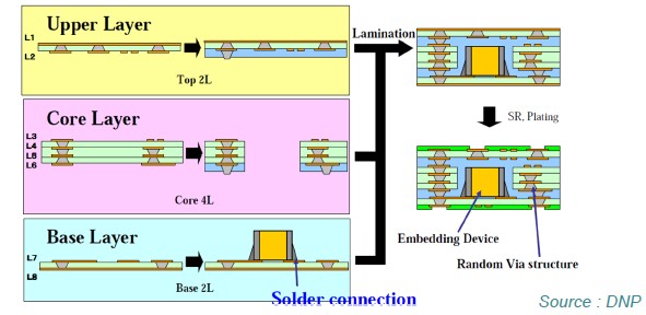
Bruce Su of ASE presented chip embedding as a technology evolution after bumping. ASE is developing "advanced Embedded Assembly Solution Integration" or aEASI as shown below:


EASI currently has the following design rules:


For all the latest on 3D IC integration and advanced packaging stay linked to IFTLE..........

Sunday, October 2, 2011

IFTLE 69: Cell phones and memory consolidation

The cellphone continues to pull in the functionality of digital cameras, PDAs, GPS navigators, mobile TV and numerous other applications. It is quickly becoming thedominant market driver for virtually all of these functions.

Earlier this summer market research firm Forward Concepts issued a report, "Cellular handset and chip markets '11: An in-depth analysis of cellphones and their chips," which indicates that cellular handset shipments grew 12% in 2010 to 1.5 billion units. It includes some interesting points that those in high end packaging should study carefully.

As we know, smartphones are expected to grow at an accelerated rate (15.4%) to the 318M unit level this year. The report provides extensive forecasts for all handset types and virtually all cellphone chips through 2015. Though Samsung and Apple are growing faster, Nokia continues to be the leading handset vendor. Nokia's average handset selling price is among the lowest because of their huge share of the low-end markets in China, India and Africa. Nokia is still the largest vendor of smartphones, but Apple is catching up, as illustrated in the graph below:


In terms of chip revenue coming from cellular handsets, Qualcomm remains the "big dog" with 23% of the market. If we include TI, Infineon and ST-Ericsson, we can account for more than 50% of the chip revenue in this market:


From the chart below we see that the display, the baseband chip and the image sensor account for more than 50% of the component value:


Predicting memory supplier consolidation

Anyone following the goings-on in the 3D IC market space would have to agree that Elpida has been at the forefront of the technology [see IFTLE 67] Several of these 3D practitioners such as Elpida, Samsung, and Micron (Aptina) also are in the memory business. A recent article attributed to Bloomberg Business Week [link] proposes that memory chip-makers ProMOS Technologies, Powerchip Technology and Elpida Memory, "burdened by debt, losses and falling prices, are under increasing pressure to seek mergers or exit the industry."

Reportedly, Elpida, which is $4.6B in debt, is "producing chips that sell for less than they cost to make." Micron, market leader Samsung, and Hynix Semiconductor are the only DRAM makers among the top eight generating a profit. DRAM makers as a group have lost 19% of their market value this year, according to Bloomberg, which quotes a financial analyst's doubts: "I find it difficult to believe they [Elpida] are going to survive this downturn [...] Consolidation is inevitable for survival in this industry."

The Japanese government's interest in maintaining an on shore supply of memory chips might limit who can acquire Elpida. Toshiba is thought of as a logical choice if such a merger is required.

According to recent announcements, Elpida Memory is considering cutting back production at its Hiroshima facility and sending more work to Taiwan partner Rexchip, its JV with Powerchip [see "Elpida shifting output to Taiwan, blames yen and ASPs]. Reports indicate up to 40% of Elpida's domestic capacity (50,000 wafer/month, 300mm wafers) could go to Rexchip would be producing the majority of Elpida's output. The Taiwan partner would produce commodity DRAM, while the Elpida Hiroshima plant would focus on memory for smartphones, according to the Nikkei daily.

No matter the outcome, IFTLE hopes these business issues do not impact the outstanding work Elpida is doing in 3D IC.

Next week we will finish updates from SEMICON Taiwan.

For all the latest on 3D IC and advanced packaging stay linked to IFTLE..........

Saturday, September 24, 2011

IFTLE 68 2011 Semicon Taiwan SiP Global Summit Part 2. 3DIC Technology and Test

The SiP global summit was held recently in Taipai. Last week we looked at the some of the 3D technology forum. This week we will finish up on 3D technology and look at highlights of the 3D Test forum "Test Challenges and Solution in the New Era of Heterogeneous Integration," chaired by Mike Liang, president and CEO of KYEC. Multiple Packaging and Testing challenges must be met to meet the production yields required to take 3D from concept to commercialization. It is crucial that the entire supply chain of material suppliers, design houses, test equipment suppliers, and package and testing houses partner to develop cost-effective test mythologies and strategies.

Victor Peng, SVP at Xilinx, updated the audience on their ongoing commercialization of Xilinx 7V2000T FPGA with their "stacked silicon interconnect technology" (SSIT).The company's FPGA 28nm slices are assembled "side by side" on a silicon interposer with 65nm interconnect wiring. They found the interposer was an excellent way to handle the 28nm chip low-k fragility.Chip fabrication, interposer fabrication and bumping is being done by TSMC. Chip bumping and module assembly is being done by Amkor.


Peng reports that Xilinx is on schedule for sampling in calendar year 2011. Peng also noted that the company "believes in full 3D IC stacking (no interposer)" but that it will take a little longer for that technology to become standardized in the infrastructure.


Recall in IFTLE 62 I discussed the nomenclature confusion part of which was "stereoscopic 3D" being confused with 3D IC. [ see IFTLE 62, "3D and interposers: Nomenclature confusion"] Well, I never thought I would see a presentation about 3D IC being used for stereoscopic 3D but that's just what happened when Taiji Utaka, SVP of technology platforms at Sony discussed the incorporation of 3D IC chips into the stereoscopic 3D Sony PlayStation. Sony is looking at the potential of improving 3D image quality by using 3D IC memory to increase performance (pixel fill rate improved by higher bandwidth) and improve latency. Sony sees the major impediment to using 3D IC as current cost, but also includes test protocol, thermal performance, proven reliability, standardization, and the availability of multiple suppliers as issues that need to be improved. Utaka interestingly noted that "game machines are required to have longer lifetime than PCs."

Jim Walker, VP of semiconductor Manufacturing for Gartner during his presentation "Going Vertical" looked at "register DIMM" used in servers comparing the newly announced Samsung 32Gb DDR3 DIMM with through-silicon vias (TSV) to previous 32Gb RDIMM. He finds the TSV-based products operate at lower power and higher speed:

-- Lower power: 4.5 Watts = 30% less than current 32Gb RDIMM without TSV
-- Higher Speed: 1333 Mbit/sec vs. 800 Mbit/sec previous 32Gb RDIMM

Eric Beyne of IMEC sees the current market divided into the following segments:

Mobile consumer applications

Memory/logic stacks:
- Increased memory bandwidth, low power
- Analog-logic stacks: Heterogeneous technology choices

High-performance applications:
- Very high memory bandwidth requirement
- Very high power processor devices
    3D SI interposer substrates

High density memory stacks:
- High bandwidth, low power DRAM

Microsystem integration:
- Combining advanced logic and memory technologies with heterogeneous device technologies such as analog, sensor, actuator, MEMS

Beyne concludes that it is difficult for designers to actually use the technology due to too many unknowns, and lack of 3D-EDA. The numerous technology options create a complex supply chain and make it difficult for equipment, material and EDA tool suppliers to develop the appropriate solutions. Thus, Beyne indicates that standardization is needed immediately in: 3D technology, 3D test, and 3D design.

Roger Hwang, director of test at ASE, noted that test must be built into the 3D TSV assembly flow at the OSAT.


At ASE, logic die will be tested after being mounted onto the substrate "strip" before singulation, and memory will be tested after tape and reel. Another test will be done to the final package after chip-to-chip bonding.


Interposer test will be done after backside processing and after film frame mounting.


Greg Smith of Teradyne listed the following unique TSV fault types:

Faults can occur in the TSV itself:
  • Voids (High resistance)
  • Oxide pinholes (short to substrate)

Faults can occur from bonding:
  • Contamination of bond surface
  • Misalignment
  • Height variation
  • TSV shorts

Faults can occur from wafer thinning:

  • I-V degradation
  • Shifts in device performance

For all the latest in 3D IC and advanced packaging stay linked to IFTLE.........