Continuing with key presentations from the 2012 IMAPS Device Packaging Conference in Ft McDowell AZ.
Tezzaron Process TechnologyBob Patti showed off two Centip3De, a 3-D IC stack using 128 ARM Cortex M3 cores and 256 Mbytes of stacked DRAM from the Univ of Michigan and the 3-D MAPS, a massively parallel processor using 64 custom cores stacked with a block 256 kilobytes of scratch pad memory from Ga Tech. For more details on these see IFTLE 93, "2.5/3D at the 2012 ISSCC".
(Click on any of the images below to enlarge them.)
Amkor's Ron Huemoeller reported that 3D vertical stacking is:
- memory and application processor driven
- today focused on 28 nm CMOS and moving to 22 nm
- application processors are near exclusively moving to OSAT finished wafer process flows
- today focused on 28 nm CMOS and moving to 22 nm
- application processors are near exclusively moving to OSAT finished wafer process flows
Whereas 2.5D Interposers are:
- network, CPU and GPU driven........ mother boards reduced from 10 to 6 layers
........ reduce chip mask layers
........ smaller x, y dimensions
- focused on large package bodies (40 -90 mm , near retical sized Si)
- both foundry and OSAT wafer flow processes being used
He sees both dis-integration of large logic blocks and separation of functions
- allows focus of specific functions which require leading process nodes
- improves wafer yield
- reduces time to market
- reduces mask layer count at advanced process nodes
Concerning the interposer supply chain:- improves wafer yield
- reduces time to market
- reduces mask layer count at advanced process nodes
- laminate (which can theoretically be delivered in large panel format (i.e. 500 x 500 mm ) are being investigated by several "elite substrate manufacturers" [ Unimicron, DNP, Shinko, Kyocera]. Limited to 8 um L/s and 40 um vias on 85 um pads today. 5 um l/s will require stepper and better resists which change the economics. 5 um L/S thought to be many years away. Latency issues will limit adoption as will limitations in va/pad design rules.
- glass can be delivered in large panel or wafer format. Several glass companies [Hoya, Corning, AGC] are investing in capability to support glass interposer technology. Glass faces challenges for CMP / damascene processing.- silicon in 200 or 300 mm several companies supporting silicon interposers in idle foundry space on legacy node technologies. Amkor finds only 3 foundry players committed to delivering "fine featured" interposers [ TSMC, GF, UMC] with TSMC the only one currently delivering in any quantity.
According to Amkor several foundry sources are interested in manufacturing Si interposers and a couple are already delivering fully functional wafers. Currently design rules "are aggressive" i.e. less than 2 um L/S and 5 um vias. Amkor indicated that the predominant interposer designs are what IFTLE has been calling "fine featured" as follows:
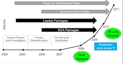
TI has recently announced that all 7 TI internal assembly and test sites are now converted to Cu WB. 6.5B devices have been shipped in Cu WB with conversions continuing. TI which started their Cu WB studies in 2003 are in HVM at the 65 node and have qualified down to the 45 node. 50% of all their interconnect wire is now Cu.
Analog, wireless and embedded products in BGA and leadframe packages are all qualified. Cu shows less wire sweep during package molding and since it has better inherent thermal conductivity it shows better battery life. Next TI will be looking at "high rel" applications such as automotive, military and down hole drilling with Cu wirebonding.
For all the latest in 3DIC and advanced packaging stay linked to IFTLE...................


No comments:
Post a Comment