Electromigration
The recent interest in electromigration is due to a number of issues including the drive to Pb free bumps, the trend towards increased IO density resulting in smaller and finer pitch bumps, and the introduction of 3D IC structures. The concurrent increase in power density is requiring chip-to-package interconnect to carry more current per interconnect. Since electromigration reliability is a direct function of interconnect dimensions and metallurgy, any new interconnect developments need to be characterized for electromigration reliability.
Solder composition and under bump metallization (UBM) are key factors that are known to affect electromigration failure. It is well known that increasing current density has a negative impact on electromigration. Reduction in bump size leads to an increase of current density with current density increasing as a square function of the bump diameter.
Yoo of Nepes reported on their investigation of the impact of UBM (under bump metallization) on electromigration for copper pillar bumps (CPB) and various UBM metallizations (Cu 5μm UBM, Cu 10μm UBM, Cu/Ni UBM ) in conjunction with SnAg solder bumps of various sizes, at a constant current density of 5.09x10⁴A/cm2.
MTTFs, obtained from Weibull plots are summarized in the Table below. MTTF (20% resistance increase) became longer as test temperature was lowered for each bump structure. At 150 C, MTTF followed the order: CPB > Cu/Ni > Cu 10μm > Cu 5μm. Life time of CPB was 35times longer than Cu 5μm UBM/solder bumps under the same conditions.
Syed of Amkor shared their studies on the factors affecting electromigration and current carrying capacity of flip chip and 3D IC interconnects. The figure below shows a Weibull failure plot for 700mA, 150C condition. High Pb failed first followed by SnPb and then SnAg bumps. As of 10,000 hrs no Cu pillar EM failure had occurred indicating the Cu pillar bumps performed much better than the other solder bump options tested. High Pb bumps are normally considered very robust in terms of electromigration performance but in this case the surface finish of the substrate is copper SOP (solder on pad) rather than the previously studied ENIG finish.
FAN OUT LP
Fan out or embedded wafer level packaging (e-WLB) remains a red hot packaging topic only rivaled by 3D IC. [ see IFTLE 22, “Sources for Fan Out WP Continue to Expand” ] In the opinion of IFTLE, FO-WLP is this decades BGA and we will see it replacing the BGA format in many application spaces. While the last decade saw the explosive growth of fan in WLP, FO-WLP takes over as a WLP technology when the package size must be larger than the chip size in order to provide a sufficient area to accommodate the 2nd level interconnects.
One of the most well known examples of FO-WLP is the “eWLB” developed by Infineon and there consortium consisting of ST Micro, STATSChipPAC and ASE.
STATSChipPAC presented data on thermal electrical and mechanical performance. In the table below we see that thermal modeling shows that an eWLB and an equivalent FC-BGA show equivalent thermal performance.
The figure below depicts Q performance comparison of inductors made by different processes/options. An inductor made directly above an active IC has a Q peak is around 26. The same inductor made from the STATS thn film IPD (integrated passive device) process has a Q max of~ 30 whereas if made on mold compound in the FO area, its peak Q can be 35.
The figure below shows comparison of parasitic values of RLC for fcBGA and eWLB at 1GHz. For resistance, eWLB has 68% less value than fcBGA. Moreover, eWLB has 66% less inductance value and 39% less capacitance compared to fcBGA. It is mainly due to shorter interconnection in eWLB.
The two main challenges of eWLP are die shift and warpage of the molded wafer. Die shift will impact the alignment of the RDL on the pad of the die and thus the larger die shift drops the yield of RDL tremendously. The encapsulated eWLP wafer need to be handled by various equipment such as an in-line track for passivation or photoresist coating and development, a mask aligner for patterning the passivation or photo-resist, and a sputter for the metal deposition process. The equipment does not accept the molded wafer if its warpage is too high. Themo-Moire technology was used for measure package warpage with temperature profile. There was study of warpage behavior with different material combinations of dielectrics and molding compound material. They note that proper selection of the mold compound and the in-depth understanding of the molding process conditions will definitely minimize the warpage of the molded wafer.
Multi-die eWLB packaging technology has become a necessity to embed different functionality dies into a single package, especially for wireless and mobile phone applications. The key challenges in processing multi-die packages are:
1) change in die positions due to thermal expansion of carrier during molding and shrinking of mold compound upon cooling 2) warpage of the reconstituted wafer due to presences of multi-dies and “chip to package” ratio 3) filling of mold compound in the narrow gap between dies and 4) Meeting package and board level reliability requirements
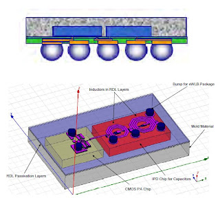
In Rf applications such as power amps (PAs) , the PA chip and a IPD can be combined into a 2 die eWLB as shown below.1) change in die positions due to thermal expansion of carrier during molding and shrinking of mold compound upon cooling 2) warpage of the reconstituted wafer due to presences of multi-dies and “chip to package” ratio 3) filling of mold compound in the narrow gap between dies and 4) Meeting package and board level reliability requirements
ST Micro, STATSChipPAC and Infineon gave a presentation on the next generation eWLB concepts. They listed the next generation variations of the eWLB as:
1) enabling two or more layers of routing
2) expanding the package size to 12x12mm
3) allowing for thinner packages and side by side chips within the eWLB
4) double sided Package on Package (PoP) eWLB
With optimized design, 12x12mm eWLB successfully passed 500 cycles of TC [40/125C, 2cycles/hr.).
Thinner packages can provide better board level reliability as well as lighter and thinner profile at the system level. eWLB can be thinned down to 250 um thickness. The critical technical challenges included handling the thin wafer and grinding and removing of the Si/epoxy material together using the same process steps. There was found more than 60% increase in thermal cycling performance with thinner eWLB and drop reliability also improved significantly.
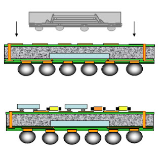
Another approach will be double sided interconnection reminiscent of the Amkor TMV structures as show below.
For all the latest in 3D IC and advanced packaging technology stay linked to IFTLE, Insights From the Leading Edge….


No comments:
Post a Comment