Friday, February 25, 2011

IFTLE 39 Packaging Roadmaps at MEPTEC

In November of 2010 MEPTEC (Microelectronics Packaging and Test Engineering Council) : a trade association of semiconductor suppliers and manufacturers)[link] brought together a group experts from AMD, Altera, Amkor, ASE, Cisco, LSI, Micron, TechSearch, Unisem , Yole and others to discuss the status of Semiconductor Packaging Roadmaps. While the presentations themselves may have had more meat on the bone, many of the handouts were short on data and long on marketing fluff or are materials that we have already recently covered. There were, however, a couple of presentations worth looking at.


Bill Bottoms, CEO of 3MTS gave the introductory talk taking a look a collaborative roadmaps and international roadmap perspectives. From his position as chair of the ITRS (Int Technology Roadmap for Semiconductors) packaging and assembly TWG (technical working group) Bill reminded attendees that ITRS is sponsored by Europe, Japan, Korea, Taiwan and the US to:


- forcast semiconductor technology requirements 15 years out and
- forcast emerging semiconductor devices and materials 10 years out


Its relationship to other Microelectronic roadmap activities in the US is shown below where i-NEMI is actually the pivot point for all the microelectronic activities.


On a global basis, the other organization looking at overall semiconductor packaging solutions is JISSO [link], a Japanese term which reflects the total packaging solution for electronic products. The chart below shows its relationship to other global standards organizations.


Bottoms premise is that for the past 40 years semiconductor progress could be easily predicted. The focus was on design and fab. Semiconductor roadmap goals were all clearly focused on shrinking geometries (scaling) and increasing wafer size. However, as we enter the “deep submicron” era, however, things become more complicated and packaging becomes a more important in delivering semiconductor yield, reliability and performance.

The answer developed to adress the historical lack of package scaling to match IC scaling was to generate the packaging at the wafer level, i.e. wafer level packaging or WLP. WLP, now firmly entrenched as a packaging option offers portable consumer products :


- inherently lower cost
- better electrical performance
- lower power requirements
- smaller size


Several architectural variations of WLP are in use today as are shown below.
Another important trend in packaging is the incorporation of multiple die into a single package or what has become known as System in Package (SiP) [ MCM to those of us that have been around awhile].
Moving forward, Bottoms predicts, as many of us do, that the 3rd dimension will be the key enabler in maintaining the “price elastic growth of the electronics industry”. While 3D presents many challenges they all appear to have reasonable solutions. 3D will appear first through silicon interposers with through wafer connections and then through chips fabricated with internal TSV for through wafer connections .

Bill updated attendees with where the packaging roadmap would be increasing and expanding coverage in 2011. [ see “Packaging, assembly changes coming in next ITRS Update” ]


Bottoms concludes that the pace of change in packaging technology has never been greater and roadmaps are critical to continuation of this rate of progress.


Bryan Black of AMD looked at why 3D is required if semiconductor technology is to continue to move ahead. In standard fashion Black defines 3D technology in two varieties as shown below, TSV in active devices and TSV on interposers.


From a systems standpoint Black proposes the interesting perspective that performance density drives new form factors, new form factors discover new usage models and without new form factors the industry would stagnate. This trend is shown in the slide below:


For all the latest on 3D integration and advanced packaging stay linked to IFTLE…..


Saturday, February 19, 2011

IFTLE 38 ...of Memory Cubes and Ivy Bridges - more 3D and TSV

The 3D TSV announcements keep coming at a “fast and furious” pace and are becoming hard for all of us to keep up with. One announcement (this past week) and one rumor, are very important for the forward momentum of 3D IC integration.


A few weeks ago Mark Durcan, COO of Micron, at the IEEE ISS meeting in Half Moon Bay, commented that Micron is ''sampling products based on TSVs” and that “Mass production for TSV-based 3-D chips are slated for the next year or 18 months'' [see IFTLE 33, “ Micron 3D Response, Sematech Standards, Leti 300 mm Line” ]

Now, Micron has announced that it is using TSV technology to address the longstanding problem referred to as the "memory wall". [see “Micron to reveal tech it says increases chip speed 20-fold” ]


For those that are interested, the seminal paper in the area appears to be “Hitting the Memory Wall: Implications of the Obvious” by Wulf and McKee in the March 1995 issue of Computer Architecture News which can be read here [link]. It presents an interesting discussion of the bounds on processor performance imposed by memory performance. Historically, processor performance has improved by about 60% per year, whereas the corresponding improvement in memory access time has been less than 10% per year. Latencies are dominated by DRAM access times which has changed VERY slowly over last 20 years. DRAM performance is constrained by the capacity of the data channel that sits between the memory and the processor. No matter how much faster the DRAM chip itself gets, the channel typically chokes on the capacity. Systems are not able to take advantage of new memory technologies because of this latency issue.

Brian Shirley, vice president of DRAM Solutions at Micron claims that their “hyper memory cube” technology “…offers a 20-fold performance increase while reducing the size of the chip and consuming about one-tenth of the power”. They reportedly accomplish this by stacking memory on top of a controller layer (shown in the Micron fig below as logic layer) and connecting with TSV. The “wide bus” from the controller layer to the CPU is reportedly “hugh” (possible 512 bits ??)


Shirley commented “Performance needs are most dire in networking and cloud computing. One-hundred gigabit Ethernet routers and switches and cloud computing servers require everything they can get……this is our way of giving them a fire hydrant.”


They hope to see the memory cube technology in server and networking markets as early as 2012, with significant volumes in 2013, and could then start to work their way toward the consumer space in 2015.


The overall concept of the control layer reminds IFTLE of the structures that Bob Patti of Tezzaron has been showing for the past 5 years (see below)


The Intel Ivy Bridge Processor is the 22 nanometer die shrink of the 32 nanometer Sandy Bridge which is expected to be commercialized in late 2011 or early 2012. Ivy Bridge is expected to pack low-power, low-speed, but large bandwidth memory (some report up 512 bits).


Although Intel will not confirm, rumors persist that the key to Ivy Bridge’s reported performance is its stacked memory and silicon interposer [see: “Intel puts GPU memory on Ivy Bridge” ]


Rumors are that Ivy bridge will use LPDDR2 memory, possibly with a speed of only 1066MHz, and that memory stacking technology could bring it up to 1GB. The memory is then stacked upon a silicon interposer. The reason a silicon interposer is essential for Ivy Bridge is the large width of the low-power memory. Since 512 bit brings with it high pin and trace counts, which would require more layers and increase cost. The interposer decreases the required on chip layers and reducing the overall cost.


IFTLE has taken the rumors a step further. IFTLE thinks it is possible that the following patent application [ see: US 7,841,080 B2 ] entitled “Multichip Packaging using an Interposer with Through Vias” which describes having a CPU on an interposer with stacked DRAM and a voltage regulator may be related to the Ivy Bridge implementation.


Ivy Bridge may be Intel’s first product introduction with TSV. We’ll know for sure one they release the information and/or once Ivy Bridge is released and analyzed by someone like Chipworks.


One additional comment. It is likely that the use of an interposer (if true) reveals that Intel agrees with Xilinx [ see: IFTLE 23, “Xilinx 28 nm Multidie FPGA…” ] and indeed true 3D stacking (memory directly bonded to logic circuits with TSV) is not yet available and/or ready for “prime time” ….yet.

For all the latest in 3D integration and advanced packaging stay linked to Insights from the Leading Edge….


Saturday, February 12, 2011

IFTLE 37 Advanced Packaging at Singapores EPTC

Like the IEEE ESTC meeting held in Europe [see IFTLE 26 Adv.Pkging at the 2010 ESTC] , Asia’s IEEE EPTC meeting, held every year in Singapore, is a sister meeting of the IEEE ECTC.

Electromigration
The recent interest in electromigration is due to a number of issues including the drive to Pb free bumps, the trend towards increased IO density resulting in smaller and finer pitch bumps, and the introduction of 3D IC structures. The concurrent increase in power density is requiring chip-to-package interconnect to carry more current per interconnect. Since electromigration reliability is a direct function of interconnect dimensions and metallurgy, any new interconnect developments need to be characterized for electromigration reliability.
Solder composition and under bump metallization (UBM) are key factors that are known to affect electromigration failure. It is well known that increasing current density has a negative impact on electromigration. Reduction in bump size leads to an increase of current density with current density increasing as a square function of the bump diameter.

Yoo of Nepes reported on their investigation of the impact of UBM (under bump metallization) on electromigration for copper pillar bumps (CPB) and various UBM metallizations (Cu 5μm UBM, Cu 10μm UBM, Cu/Ni UBM ) in conjunction with SnAg solder bumps of various sizes, at a constant current density of 5.09x10⁴A/cm2.
MTTFs, obtained from Weibull plots are summarized in the Table below. MTTF (20% resistance increase) became longer as test temperature was lowered for each bump structure. At 150 C, MTTF followed the order: CPB > Cu/Ni > Cu 10μm > Cu 5μm. Life time of CPB was 35times longer than Cu 5μm UBM/solder bumps under the same conditions.

Syed of Amkor shared their studies on the factors affecting electromigration and current carrying capacity of flip chip and 3D IC interconnects. The figure below shows a Weibull failure plot for 700mA, 150C condition. High Pb failed first followed by SnPb and then SnAg bumps. As of 10,000 hrs no Cu pillar EM failure had occurred indicating the Cu pillar bumps performed much better than the other solder bump options tested. High Pb bumps are normally considered very robust in terms of electromigration performance but in this case the surface finish of the substrate is copper SOP (solder on pad) rather than the previously studied ENIG finish.
FAN OUT LP


Fan out or embedded wafer level packaging (e-WLB) remains a red hot packaging topic only rivaled by 3D IC. [ see IFTLE 22, “Sources for Fan Out WP Continue to Expand” ] In the opinion of IFTLE, FO-WLP is this decades BGA and we will see it replacing the BGA format in many application spaces. While the last decade saw the explosive growth of fan in WLP, FO-WLP takes over as a WLP technology when the package size must be larger than the chip size in order to provide a sufficient area to accommodate the 2nd level interconnects.

One of the most well known examples of FO-WLP is the “eWLB” developed by Infineon and there consortium consisting of ST Micro, STATSChipPAC and ASE.


STATSChipPAC presented data on thermal electrical and mechanical performance. In the table below we see that thermal modeling shows that an eWLB and an equivalent FC-BGA show equivalent thermal performance.

The figure below depicts Q performance comparison of inductors made by different processes/options. An inductor made directly above an active IC has a Q peak is around 26. The same inductor made from the STATS thn film IPD (integrated passive device) process has a Q max of~ 30 whereas if made on mold compound in the FO area, its peak Q can be 35.


The figure below shows comparison of parasitic values of RLC for fcBGA and eWLB at 1GHz. For resistance, eWLB has 68% less value than fcBGA. Moreover, eWLB has 66% less inductance value and 39% less capacitance compared to fcBGA. It is mainly due to shorter interconnection in eWLB.
The two main challenges of eWLP are die shift and warpage of the molded wafer. Die shift will impact the alignment of the RDL on the pad of the die and thus the larger die shift drops the yield of RDL tremendously. The encapsulated eWLP wafer need to be handled by various equipment such as an in-line track for passivation or photoresist coating and development, a mask aligner for patterning the passivation or photo-resist, and a sputter for the metal deposition process. The equipment does not accept the molded wafer if its warpage is too high. Themo-Moire technology was used for measure package warpage with temperature profile. There was study of warpage behavior with different material combinations of dielectrics and molding compound material. They note that proper selection of the mold compound and the in-depth understanding of the molding process conditions will definitely minimize the warpage of the molded wafer.
Multi-die eWLB packaging technology has become a necessity to embed different functionality dies into a single package, especially for wireless and mobile phone applications. The key challenges in processing multi-die packages are:
1) change in die positions due to thermal expansion of carrier during molding and shrinking of mold compound upon cooling                                             2) warpage of the reconstituted wafer due to presences of multi-dies and “chip to package” ratio                                                                                   3) filling of mold compound in the narrow gap between dies and                   4) Meeting package and board level reliability requirements
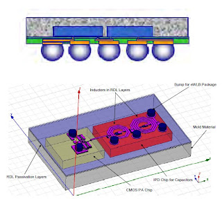
In Rf applications such as power amps (PAs) , the PA chip and a IPD can be combined into a 2 die eWLB as shown below.
ST Micro, STATSChipPAC and Infineon gave a presentation on the next generation eWLB concepts. They listed the next generation variations of the eWLB as:

1) enabling two or more layers of routing
2) expanding the package size to 12x12mm
3) allowing for thinner packages and side by side chips within the eWLB
4) double sided Package on Package (PoP) eWLB


With optimized design, 12x12mm eWLB successfully passed 500 cycles of TC [40/125C, 2cycles/hr.).
Thinner packages can provide better board level reliability as well as lighter and thinner profile at the system level. eWLB can be thinned down to 250 um thickness. The critical technical challenges included handling the thin wafer and grinding and removing of the Si/epoxy material together using the same process steps. There was found more than 60% increase in thermal cycling performance with thinner eWLB and drop reliability also improved significantly.

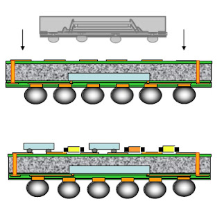
Another approach will be double sided interconnection reminiscent of the Amkor TMV structures as show below.


For all the latest in 3D IC and advanced packaging technology stay linked to IFTLE, Insights From the Leading Edge….


Friday, February 4, 2011

IFTLE 36 3D IC at the RTI ASIP part 2

Continuing our look at activities at the RTI 3-D Architectures for Semiconductor Integration and Packaging Conference ( 3D ASIP) held in Dec 2010 in Burlingame CA.
Hiroaki Ikeda (Elpida), Tae-Je Cho (Samsung) and Mitsumasa Koyanagi (Tohoku Univ) discuss the future of 3D IC technology with IFTLE’s Garrou
Sungdong Cho – Samsung

Songdong Cho, Sr engineer in the Samsung system LSI group spent the conference besieged by questions from attendees on the Samsung (memory group) announcement that occurred the day before the meeting. [see IFTLE 27, “The Era of 3D IC Has Arrived with Samsung Commercial Announcement”]


Cho first led the attendees through the evolution of Samsung 3D IC technologies:


- 2006 Samsung announces memory stacking technology


-2007 DRAM stacked memory package using TSV


-2008 TSV for CMOS image sensors mass production


- 2008 memory + logic on silicon interposer – start development


-2010 announce DRAM stacked memory with TSV commercialization


(all of these can be found in past editions of PFTLE and IFTLE)


Cho indicated that mobile products will require more than 25 GB/sec bandwidth in ~ 2012 and therefore “..wide I/O memory with TSV is the only solution” There will be two platforms for the systems LSI group: Interposer and memory on logic as shown below.
They are developing 6 x 50 copper TSV middle technology with O3 TEOS liner . Their process flow is shown below:
During process development they have dealt with the following challenges:

- High AR TSV filling
- Cu extrusion
- Stress impact on devices
-Copper contamination (through sidewall and during backside processing)


By eliminating voids during the plated copper filling they were able to achieve 99.57% via chain yield.


Cho lists (3) ways to deal with Cu extrusion:


- Tungsten TSV
- Cu TSV last backside
- Via size and depth reduction


They have determined a workable depth vs diameter space using the 3rd option which results in less than 0.2 um extrusion. [ recall this was first shared with us by Bob Patti – see PFTLE 53, “You Can’t Always Get What You Want”]


They worry about copper contamination when backside processing due to a decrease in the gettering layer (see previous discussions in PFTLE 117, “On copper diffusion, gettering and the denuded zone”]


Cho indicates that they will not use W because of the severe wafer bow that even 1 um of W imparts to a 300 mm wafer. They also see severe Si cracking and IMD cracking due to the high W stress.
Cho expects to see mass production from his side of the business in 2013.


Eric Beyne - IMEC


Conference co-chair Eric Beyne, program director for advanced packaging and interconnect at IMEC . The IMEC standard processes have been discussed several times previously [ see PFTLE 122, “3-D IC at the IEEE ISSCC” ; PFTLE 93, “ Semicon TechXPOTs” ]


Beyne indicates that high speed graphics applications are demanding 512 GB/sec memory bandwidth and thus agrees with the consensus that 3D with TSV is the only way to go.


The POR for their 3D TSV middle process (3D-SIC) is 5 x 50 um which looks like it is becoming an industry standard.


Their wafer thinning technology achieves a less than 1.6 um TTV for a 300 mm wafer thinned to 50 um.
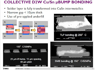
Their Cu/Sn micro bump bonding technology is currently at 25 um bumps on 40 um pitch.
Jean-Marc Yannou – Yole Developpment


Yannou focused on the use of 3D interposers for 2.5D technology and offered the following proposed interconnect gap timeline showing that silicon / glass interposers offer 10x more resolution and finer pitches than traditional organic substrates.


Yole reports that they have found 8 categories of applications for silicon / glass interposers as shown below:

Arif Rahman – Xilinx


Arif Rahman, principle engineer at Xilinx gave further details on their next generation FPGA choices that have been reported recently [ see IFTLE 23 , “Xilinx 28 nm Multidie FPGA…”]


When asked about their choice of a silicon interposer for their next generation FPGA, Arif Rahman commented that “ it appeared to be the most manufacturable way to offer product performance during our required timeline” which I interpret as “”full 3D is not quite to the point that we were ready to bet the farm on it”


The interconnect on the interposer is done at 65 nm technology. In terms of scalability Rahman noted that the technology was currently limited by “…how big an interposer you can get”

Note: After the conference Arif left word that he had moved to Altera - interesting !


Larry Smith - Sematech


In their 3D program update, Smith indicated that after much study and consultation with its members, Sematech was focused on 5 x 50 um copper vias middle with AR = 4-10 and pitch of 10-50 um. Their status assessment is shown below:

Paul Enquist - Ziptronix
Ziptronix highlighted their program with Kodak which produced a 1.5 MPixel BSI (back side imaging) CMOS Image sensor with 1.25 um pixel pitch as shown below.
NOTE: For those not paying attention, ZIptronix has filed patent infringement charges against TSMC and Omnivision [see "Ziptronix accuses Omnivision, TSMC of patent infringement"
Lisa McIlrath – R3Logic

Lisa McIlrath, CEO of R3Logic was one of the first to understand and tackle the EDA requirements of 3D IC technology. [ see PFTLE 102, “The Four Horseman of 3D IC” ]


She had what was probably the quote of the conference when she astutely stated “3D Integration will become mainstream when it is the best economic alternative” Simple yet accurate ! From her design perspective she feels that this will occur by maximizing IP re-use.


Philippe Royannez - IME


IME 3D technology has been discussed previously [see PFTLE 98, “ TSMC Confirms 3D Intent / Singapore Launches 3D IC Consortium “ ]


Philippe Royannez, Director Sytem & Digital IC at A-STAR updated activities at IME in Singapore. Royannez indicates that their 300 mm line will be fully operational n the 2nd- 3rd quarter of 2011.


In keeping with the cost reduction theme, Royannez indicated that IME “ has solutions to most of the technical challenges now. The real focus now needs to be making these solutions low cost. “


When it comes to EDA Royannez notes that “designers understand the theoretical benefits of TSV but cannot quantify it precisely and don’t quite understand what to do to use them” He notes that 3D IC EDA flow “is more evolution than revolution…all the ingredients are there” but then quickly added “..for true 3D IC, that is the spreading of blocks across layers, certainly we’re not quite there yet, but for initial 3D programs we are in pretty good shape”


In an interesting blood pressure monitor application Royannez made the point that we need to be focused on system level integration. In this application shrinking the size of the circuits and making them faster will not have any impact on the size of the battery which will continue to drive the overall size of the device.


Tzu Kun Ku - ITRI


The ITRI Ad-STAC ( Adv Stacked system Technology and Applications) program has been detailed previously [see PFTLE 105 “Taiwanese Focus on 3D IC”]


The ITRI 3D program currently covers both chip stacking with TSV and the use of 3D interposers. There are currently 120 technologists assigned to their program (80 design, 40 process development). Their TSV formation roadmap is shown below. Their 300 mm line is in place and their baseline process is scheduled to be completed end of this year.

Of interest is their slide on the benefits of interposers shown below:

For all the latest in 3D IC and advanced packaging stay linked to IFTLE, Insights From the Leading Edge…