Saturday, March 26, 2011

IFTLE 43 IMAPS Device Packaging Highlights – 3DIC

Ft McDowell AZ was once again the site of the IMAPS Global Business Council Meeting and Device Packaging Conference. For a report on last years conference see PFTLE 123,125,126 [link]


Brandon Prior of Prismark Partners pointed out that 3D TSV will be competing with the incumbent mobile phone 3D packaging solutions, PoP and PiP. PoP lacks the ability to interconnect more than 200 – 300 I/O from memory, but offers ease of test. TSV will offer higher speed and many more connections .


James Malatesta of Micron presented his perspective on the work of JEDEC committee JC63, the multichip package committee. First PoP changed the landscape as logic suppliers realized that standard top package “memory modules” were requuired for multiple industry supply sources. He also gave an interesting comparison of low power DDR2 [LPDDR2] vs the wide IO TSV technology that is expected to replace it [see IFTLE 40, “Samsung Wide I/O DRAM for Mobile Products…”]

Sitaram Arkalgud, Director of Sematechs 3D IC program described their current acivities on the U Albany campus. They view their role as helping to :

• Develop robust technology solutions
• Assist member company implementation
• Drive convergence of the materials/equipment solutions


Sematech has examined the current 3D TSV tool set and come to the following conclusions:

Rosalia Beica of Applied Materials announced that EMC 3D has achieved their goal of less than $150 / Wafer for 3D processing.

In Matt Nowak, Sr Director at Qualcomm, presentation he asked the question “since the key attributes of 3D IC are: (1)Performance enhancement; (2) Improved power efficiency; (3) Form factor miniaturization and (4) Cost reduction can 3D IC take the place of scaling as CMOS technology appears to be slowing down or stalling out” . He concludes:

• If performance enhancement and power reduction are the primary motivation, then TSS opens new opportunities for innovative architectural and SW solutions with major improvements possible. But requires Pathfinding and risk taking.
• If form factor miniaturization is the only motivation, then yes
•If cost reduction is the primary motivation, then generally the answer is no. However, TSS can provide cost reduction within a window of time for large die sizes on leading edge nodes.
• If cost improvement from CMOS scaling diminishes in future nodes (due to Adv Litho and FEOL cost), then the window of opportunity for TSS increases.


Taiji Sakai of Fujitsu made a strong case for why low pitch bonding has moved to copper pillar bumps and wants to move to direct Cu-Cu bonding . The limiting factor preventing that move right now is time/temp required.
Sakai reports that if the Cu bumps are cut (planed) with a diamond bit a surface Ra of 7 nm is obtained and an “amorphous like layer” is produced at the surface. Forming a monolithic interface is possible at 200 – 250C (30 min) vs the 350C (30 min) required for a CMP’ed surface.

3D Panel Session
The 3D panel session was put together by Qualcomm’s Matt Nowak and moderated by Applied Materials Paul Siblerud.

Interposers failing thermal cycling tests


It was the fall of 2009 that everyone became aware of copper protrusion (or pumping ) as a reliability issue in 3DIC technology. This was discssed extensively in last years IMAPS DPC[ see PFTLE 125, "3D IC at Ft McDowell"] . In the last 12 months many major players confirmed the issue, solutions were proposed and our fears were allayed as to this being a showstopper for 3D IC technology [see IFTLE 6, "Cu-Cu and IMC Bonding Studies at 2010 ECTC"; IFTLE 30, "IEEE 3DIC 2010 in Munich" and IFTLE 34, "3D IC at the 2010 IEDM" ].


The rumors going around at this years IMAPS-DPC were concerned with interposers reportedly failing thermal cycling (TC) reliability tests. Word has it that when the interposers are populated with unequal size or thickness silicon chips or stacks the stresses generated on the interposers is so significant that it causes interposer fracture. I asked the panel, which I was part of, to comment on these rumors. Ron Huemoeller, VP of 3D packaging for Amkor answered that this indeed was the case, that they had seen such problems in the Xilinx scaleup. The good news from Ron is that they were able to engineer around these issues. FYI, recall that the Xilinx interposer is 100 um thick. It is unclear from the current rumors at what thicknesses (chips, stacks and interposers) these issues are seen.


Underfill with Interposers


Underfill has been around since Tsukada told us that they allowed bumped chips to reliably be used on laminate substrates back in 1992. Thus, one would think that underfills would not crop up as a problem in todays 3D technology. However, you must recall that for something like the Xilinx structure [see IFTLE 28, "Xilinx 28 nm Multidie FPGA..." we are talking about microbumps on 45 um pitch, not your typical 150 um solder bumps on 400 um pitch. Amkors Huemoeller comments on the 3D panel that the underfill process took a year get to a manufacturable state. Hopefully the underfill supplies now have the formulations set and can recommend solutions that can be implemented much quicker than that.

Phil Garrou (representing Yole Developpment), Ron Huemoeller (Amkor) Eric Strid (Cascade Microtech), Matt Nowak (Qualcomm), moderator Paul Siblerud (Applied Materials)

EMC 3D closing down…….


Paul Siblerud of Applied Materials gave the conference pre notification that EMCD 3D consortium members have concluded that they have met their goals and will be closing this summer. Their last presentation as a group is expected to be at Semicon this July.

Memory Stack Usage coming soon
Huemoeller offered the following Amkor roadmap for memory stack usage:

 Representing Yole Developpment I offered the following slide as representing the major 3D IC announcements in the past 12 months.

And the following chart to summarize active major players and their expected timelines for interposer and stack introductions.


The Latest on Xilinx FPGA Production with TSV Based Interposers

At the GBC, Suresh Ramalingam of Xilinx discussed the key role of supply chain collaboration. The FPGA is basically a programmable SoC of logic, memory and analog circuits.
Customers were asking for more logic capacity, more high speed transceivers, more processing elements and more memory and Xilinx was faced with the reality that yield of the devices is directly proportional to device size. Rather than try to interconnect smaller devices on a PWB or MCM, which did not offer enough I/O and resulted in high latency and high power usage, their preferred solution was to connect FPGA “slices” on a silicon interposer which offered massive low latency interconnect (10K routing connections between slices with ~ 1ns latency) and low power consumption. They claim this gives them a 1.9X advantage over their nearest competitor.


The 28nm Virtex-7 SSIT will reportedly use TSMC fabricated 100µm thick silicon interposers with 10 – 12 µm Cu TSV and 65nm interconnect. The micro-bumps are Cu-SnAg alloys at 45µm pitch.


The supply chain they put together includes TSMC, Ibiden and Amkor as shown below.
Mike Kelley, Sr Dir of Advanced 3D Packaging for Amkor indicated that Amkor bumped the FPGA chip wafers whereas the interposers from TSMC arrived bumped and ready for assembly.


Amkor offered the following process flow for test during assembly :

For all the latest in 3DIC and advanced packaging news stay linked to IFTLE.............





Sunday, March 20, 2011

IFTLE 42 IMAPS Device Packaging Conference – Fan Out and Embedded Packaging

Ft. McDowell AZ was once again the site of the annual IMAPS Global Business Council Meeting and Device Packaging Conference. [For reports on last years conference see PFTLE 123,125,126]

Fan out and Embedded Packaging

Andy Strandjord and Linda Ball put on an excellent panel session on fan out and embedded technology.
John Hunt (ASE), moderator Linda Ball (Freescale), moderator Andy Strandjord (Pac Tech), Thorstern Meyer (Intel Wireless [formerly Infineon]),Tom Strothman (STATSChipPAC), Lars Boettcher (Fraunhofer IZM), Navjot Chhabra (Freescale)


Thorsten Meyer one of the developers of the Ifineon eWLB fan out technology informed the audience that his group is now part of the Intel purchase of the Infineon wireless business. They are now the stand alone business “Intel Mobile Communications” Infineon retains rights to non wireless applications. Anyone wanting to license the technology moving forward will have to license from both parties.

Navjot Chhabra (recently from the Sematech ultra lowK program) is now Director of the Freescale RCP fanout technology. They are currently running a 200 mm engineering line while licensee Nepes has a 30 mm line running in Singapore. [see IFTLE 25, “IMAPS Part 2: Advanced Packaging] He indicates that qualifications for “…industrial and automotive products are ongoing”

Meyer also reveled that IZM had licensed their embedding technology (shown below) to Infineon.

Tom Strothman of STATSChipPAC indicated that eWLB is today less costly than FcBGA. STATS is currently running a 300 mm line for production of eWLB.

The panel made the interesting comment that both the fan out and embedded technologies were capable of 0.3 mm pitch but that drop test reliability would go down because the UBM cross section would be smaller.


John Hunt of ASE indicated that ASE does not have 300 mm eWLB in production but commented that “..demand just does not warrant putting that capacity in place” . It was news to me, and I’m sure it will be to most of you, that Infineon is the only commercial customer for eWLB today. Reportedly ST Micro is close but today it is only Infineon .

Much has been made of the possibility for eWLB to move to panel production. Having tried to do thin film packaging on 450 mm panels at Micromodule Systems in the mid 90’s (see fig below) I know that this is easier said than done. (FYI that’s AVX’s Bob Heistand 3rd from the left on top row, Intels Mike Skinner to the right of me and Larry Moresco in front of him. MMS program Mgr Chung Ho was absent from the
picture.


While all of the eWLB licensees are proposing fan out packaging on panels Hunt commented that “…we (ASE) are actually the only ones who have tried to do this….If we move forward with this approach it will require a totally new materials set” Hunt also indicated that they are attempting this work on ¼ panels not full PWB panels and obviously they cannot use MUF (molded underfill) to encapsulate the large substrates.

Next week we will look at a summary of 3D activity at the IMAPS DPC

For all the latest in 3DIC and advanced packaging information stay linked to Insights from the Leading Edge….


Saturday, March 12, 2011

IFTLE 41 SRC Focus Center 3D Update

Founded in 1998, the Focus Center Research Program (FCRP), is one of three research program categories of the well known Semiconductor Research Corporation (SRC) [link]. FCRP research is always looking long-term and big-picture, seeking breakthroughs that are “critical to U. S. security and economic competitiveness”. FCRP programs involve 41 universities, 333 faculty and 1215 doctoral graduate students. The Focus Centers themselves are not physical locations, but rather consist of multiple universities which engage the leading experts at the participating institutions. Each Center is managed by Center Director and addresses one of the major technology focus areas of the International Technology Roadmap for Semiconductors (ITRS).
The SRC runs 6 “focus centers” (below). All 6 centers believe 3D is important and are working in the area. On Feb 11th the first cross center 3-D workshop was held.
Tanay Karnik of Intel examined 3Dintegration from the perspective of a processor company. IFTLE has discussed the requirements for low power high bandwidth memory in several recent blogs [ see IFTLE 38, “of memory cubes and Ivy Bridges” and IFTLE 40, “Samsung Wide I/O DRAM for Mobile Products…”]. The slide below shows the bandwidth required to stay on the roadmap.

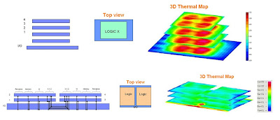
When examining thermal issues Karnik emphasized that thermal floorplanning was necessary to insure that thermal hot spots are not aligned as shown below.
In addition thermal TSV will likely be needed to carry heat directly to the heat spreader as shown below.
Jerry Bartley of IBM 3D opportunities and prerequisites to deployment. Bartley gave the following standard IBM list as 3D IC advantages:
Bartley sees an evolutionary path whereby the via diameter, via pitch, number of layers, complexity of the layers, will systematically improve with time. As we have repeatedly said here at IFTLE, Bartley sees “…3D adoption within any application will happen as the technical risks are mitigated and clear cost and performance advantages emerge”

In agreement with Intels Karnik, Bartley points towards to thermal awareness as a necessary prerequisite for 3D design as shown below.
Bartley sees 3D optimization requiring “3D thinking and system level thought processes” and lastly asks the question that a lot of us are struggling with “Is it a chip or a package ?”


Andrew Kahng of UC San Diego reviewed IRTS technology working groups which are involved with 3D technology. IFTLE has recently reviewed the same material [ see IFTLE 16, "The 2009 ITRS Roadmap.."] As an example of some of the things being looked at Kahng pointed to the prober challenges we are expected to see after 2013.

Paul Franzon from North Carolina State discussed he design of 3D systems. Franzon also identified memory on logic as a key driver for TSV based 3D architecture with examples such as high end mobile graphics synthetic aperture radar. When examining the advantages of 2D vs 3D for the synthetic aperture radar application we can see that 3D has significant advantage.
Muhannad Bakhir from Ga Tech focused on liquid cooling for high performance 3D systems. While the thermal impact of micro channel cooling can be significant, the space occupied by the liquid cooling channels is not insignificant and will limit the thinness of the strata.

For all the latest information on 3D IC and advanced packaging stay linked to Insights From the Leading Edge…….


Friday, March 4, 2011

IFTLE 40 Samsung 3D IC Wide I/O DRAM and Semiconductor Predictions for 2011

Samsung wide I/O DRAM for Mobile Applications

Samsung, who first revealed 3D TSV stacked memory prototypes in 2006, announced 40nm 8GB RDIMM based on four-gigabit, 1.5V, 40 nm DDR3 memory chips operating at 1,333MHz and 3D TSV chip stacking technology in Dec of 2010. Samsung claimed the 3D TSV technology saves up to 40 percent of the power consumed by a conventional RDIMM and improves the memory chip density. This DRAM chip was suggested for servers to reduce power consumption and save space. They said Samsung planed to apply the higher performance and lower power features of its TSV technology to 30nm-class and finer process nodes.
At the recent plenary lecture of Dr Oh-Hyun Kwon, President of Samsung ‘s semiconductor business, at IEEE ISSCC 2011 (Int Solid State Circuits Conference), he announced the development of wide I/O 1 Gb DRAM. This memory is reportedly aimed at mobile applications like smartphones and tablet computers. Kwon reports that the 3D TSV architecture will be implemented on their 50 nm node DRAM technology. In related disclosure at the ISSCC Samsung researchers offered more details about the wide I/O memory chip in their technical presentation entitled “ A 1.2V 12.8 Gb/s 2 Gb Mobile Wide I/O DRAM with 4 x 128 I/O Using TSV Based Stacking”.
Previous generations of mobile DRAMs used a maximum of 32 pins for I/O. The new wide I/O solution which has 512 I/O (up to 1200 total) pins can transmit data at a rate of 12.8-Gbytes per second resulting in a significant improvement in processing power. In addition it reportedly reduces the power consumption by 75% by reducing load capacitance. It is expected to replace low power DDR2 DRAM (LPDDR2) which runs at approximately 3.2-Gigabytes per second according to Samsung.


Following this wide I/O DRAM launch, Samsung is aiming to provide 20nm, 4Gb wide I/O mobile DRAM sometime in 2013. Traditionally "wide" parallel interfaces have been more expensive to manufacture and package. Samsung claims, however, that its 1Gb memory chip with wide bandwidth can be installed instead of a larger amount of smaller chips which results in reduced costs and higher performance.


The die area is 64.34mm2, about a 25% increase when compared with 1Gb LPDDR2. This comes mostly from the increase in number of circuits to support 4-channel and 512-DQ feature. The whole chip is made up of 4 partitions which are symmetric with respect to the chip center, and each partition consists of 4×64Mb arrays, peripheral circuits and microbumps. To reduce power consumption in 512b I/O operations and to support high data bandwidth, I/O driver loading is reduced by adoption of 44×6 microbump pads per channel, which are located in the middle of the chip. The microbumps are 20×17μm2 on 50μm pitch. A fabricated TSV has 7.5μm diameter, 0.22 to 0.24Ω resistance and 47.4fF capacitance.

Semi ISS

The SEMI ISS meeting (Industry Strategy Symposium )[link] is an annual January event in Half Moon Bay, CA where industry experts and other economic prognosticators make predictions about the upcoming year for the semiconductor industry. [ see PFTLE 121, “IC Consolidation, Node Scaling and 3D IC” for last years coverage]

Bill McClean of IC Insights pegged the 2010 semiconductor market at $313.8B, an increase of 32% over 2009. He is predicting a 10% increase for 2011. He claims a 98% increase in capex occurred between 2009 and 2010 and projects a 6% increase in 2011 to $53.8B. The semiconductor materials market saw a 24% increase between 2009 and 2010 to $42.9B and will see a 8% increase in 2011.

When looking at capex by region (2011 projected vs 2005) we see NA holding constant, Japan and Europe going down while Taiwan and Korea are going up.


10 companies held 85% of the worlds 300mm capacity in 2010.


Handel Jones of IBS predicted the following :

- 28.1% semiconductor growth in 2010 to be followed by 7.4% increase in 2011. He predicts the next downturn will be in 2013

- 32 nm is in high volume at Intel and 28 nm is ramping at the major foundries, i.e TSMC, Samsung, Globalfoundries

- Intel will ramp 22 nm in 4Q 2011, others ramping in 2012 or 2013

- process technology development is concentrated into a declining IDM and foundry vendor base

- roadmaps past 22/20 nm are unclear

- IC vendors are migrating into providing system level solutions

- A number of significant companies are making significant expenditures in 3D TSV technology with memory on package being a key driver

When looking at growth by geographic region IBS sees China becoming 50% of total consumption by 2012-2013. This means foreign supply will remain a significant portion (ca. 90%) of consumption out into he future (2015)
Reitterating his prediction of last year [ see PFTLE 121, “IC Consolidation, Node Scaling and 3D IC” for last years coverage] Jones still sees only Samsung , Intel and maybe ST Micro as IDMs with their own 22 nm logic lines. The reason for this is again explained in terms of the “cost of developing the next generation process technology” as shown below.
For the first time since we have started following the scaling roadmap, Jones sees an increase in cost / gate at the 22 node.
Thus at 28 and 22 nm taking cache off chip into a 3D technology may be a viable economic option.

For all the latest in 3D integration and advanced packaging stay linked to IFTLE…….

Hope to see many of you at the IMAPS Device Packaging Symposium in AZ next week !