Finishing up our look at the presentations at ECTC 2013 in Las Vegas.
Shinko and CEA Leti detailed their presentation
entitled “Warpage Control of Silicon Interposer for 2.5D Package Applications”.
Large silicon-interposers when attached to an
organic substrate can cause significant warpage problems. Shinko / Leti
examined several warpage control techniques including:
-
Using a “chip first process” where chips
are mounted on the interposer first
vs “chip last process” where the silicon-interposer is mounted on the
organic substrate first and chips are mounted onto the interposer last.
- using various underfill resins.
- using Sn-57Bi solder and thus lowering peak
temperature 45-90 degree C. This reduced warpage after reflow to 75% of that
using SAC305.
Comparison of warpage using different
assembly sequences is shown below.
Warpage of silicon-interposer using three
types of underfills (shown below) for 0
level assembly (micro bumps) is shown below. Maximum warpage using U.F. A1, A2
and A3 were 108, 123 and 132m, respectively. The lowest warpage was obtained
at using U.F. A1. With U.F.A3, solder bump open failures were observed. The
authors conclude that “… using underfill material with low Tg and high storage
modulus for 0 level leads to high reliability”

TSMC and customer
Xilinx presented “Reliability Evaluation of a CoWoS-enabled 3D IC Package” which
used FEA to study the thermo-mechanical response of the interposer-based
package during thermal cycle reliability stressing. Focus was especially on the
fatigue failures of the C4 and BGA joints. Experimental data collected on CoWoS
test vehicles were used to validate the FEM models. Parametric study of key
package material and geometric parameters was performed to analyze their
effects on C4 bump thermal cycle reliability. Package materials of interest
include UF (underfill), lid and substrate, and the geometric parameters include
lid thickness and C4 bump scheme.
Results showed that the CoWoS package using AlSiC lid has better C4 bump
life than the CoWoS package using Cu lid.
While a thicker lid has the
higher stiffness and better co-planarity, the higher constraint from the
thicker lid induces higher stress inside the package which negatively
impacts C4 bump fatigue and the
micro-bump Ti/Al delamination.
C4 bump layer underfill with Tg of 70 C or 120 C, were studied. The
underfill with lower Tg has higher driving force to C4 bump fatigue. When
temperature is above Tg, the underfill has much lower Young’s Modulus which has
much lower capability to protect C4 bump; and therefore the underfill with
lower Tg has higher driving force to C4 bump fatigue. On the contrary, the
underfill with lower Tg has lower driving force to Ti/Al delamination in the
micro-bump structure. TheC4 underfill with lower stiffness can play as a buffer
layer and results in lower driving force to Ti/Al delamination in microbump.
IMEC reported on “Key Elements
for Sub-50μm Pitch Micro Bump Processes”.
Scaling the ubump pitch from hundreds to a few tens of microns is not
straightforward. Several process parameters need to be taken into account to
allow a reliable Cu(Ni)Sn ubumping process. One of the challenges for fine
pitch Cu(Ni)Sn stacking is to obtain a high bump uniformity. The non uniformity
prevents Cu and Sn from having good contact and subsequent intermetallic
formation and increases the risk of underfill entrapment.
A bump scheme that offers better margin for alignment
error is better based on a scheme where the size of top die bumps is smaller
than the size of the bottom pads. For example it is better to achieve 20μm pitch with 7.5μm bump on 12.5μm pad than
with 10μm bump and pad because equal
bump and pad diameter can tolerate only 2μm misalignment whereas the 7.5μm/12.5μm bump/pad can tolerate 5μm. This
is a significant difference when working close to the stacking tool’s limit of
alignment accuracy.
Details on the plasma treatments necessary when
attempting to plate into these fine featured plating resists are also
discussed.
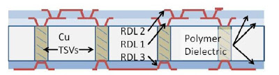
RTI
detailed a process for the fabrication and bonding of 100 and 200um thick silicon interposers with filled 4:1 AR
copper filled TSVs and front side and backside multilevel metal copper/ thin
film polymer routing layers in their
presentation ”Fabrication and Testing
of Thin Silicon Interposers with Multilevel Front side and Backside
Metallization and Cu-filled TSVs”.
For most applications, the desired thickness for Si
interposers is below the thickness at which unsupported wafers can be safely handled
through the necessary fabrication processes (i.e. 100 -200um). In these cases a
temporary wafer support system, consisting of a carrier wafer and a layer of a
temporary adhesive, must be used.
3M’s Wafer Support System (3M WSS™) and Brewer Science’s
WaferBOND 9001™ were the temporary bond materials selected in the RTI program.
Multilevel metal was done on either side of the interposer using polymer thin
film dielectrics. The front side of the device wafers was patterned with two
layers of Cu and three layers of polyimide (HD-4100 from HD Micro). After
frontside patterning, the wafers were bonded face-down to temporary carrier
wafers coated with temporary adhesive. Backgrinding and CMP were used to thin
the wafers to a nominal thickness of 100 um. After thinning, a backside Cu
routing pattern was formed between two layers of either BCB 4024-40 (Dow Chemical), HD-8930
(polybenzo-bisoxazole [PBO] HD Microsystems), with curing temperatures of 250˚C
and 200˚C, respectively, at or below the temperature limit of the temporary
adhesive. The polyimide that we used for the front side MLM structure has a
recommended cure temperature of 375 C which would be incompatible with any
currently offered temporary adhesive.
Both the 3M and the Brewer wafer bonding solutions were found
to be compatible with the processing of the different spin-on dielectric
materials used to fabricate frontside and backside MLM structures. Successful
debonding of the carriers was done both at the wafer level before dicing and at
the die level after dicing and bonding to a substrate.
In bot the 100um and
200um interposer thicknesses with 25um or 50um diameter TSV respectively, an
annealing step was found to be successful in preventing Cu from extruding from
the TSVs during the subsequent polymer curing steps. Electrical testing before
and after thermal cycling showed the high yield and stability of all of the
interposer structures irrespective of the dielectric materials choice.
For all the
latest in 3DIC and advanced packaging stay linked to IFTLE…………………..


