Sunday, May 27, 2012

IFTLE 103 2012 IMAPS AZ Device Pkging Conf; Fujitsu Low Temp Cu-Cu Bonding

It's been over for a few months now, but IMAPS was a bit slow this year gathering the presentations from their device packaging conference, This is however understandable and excusable due to the untimely death of IMAPS employee Jackie Joyner. So let's begin looking at the 2.5/3D and significant advanced packaging papers.

SSEC Wet Etch for Via Reveal
Laura Mauer of SSEC discussed silicon wafer thinning to reveal Cu TSV. The standard via reveal processis shown below. SSEC contends that a KOH wet etch process can be used for the final Si removal without etching the oxide liner. This can be sealed with oxide/nitride and then CMP'ed to expose the Cu vias.

Wet etch with HF/HNO3 has also been proposed by ASET and shown to have minimal impact on the electrical characteristics of the transistors [link].
Asahi Glass TGV (Through Glass Vias)
Takahashi of AGC discussed the fabrication of TSV in glass. They have been able to fabricate TGV with a  193 nm ArF excimer laser by using short pulse width (20-30 ns). The TGV do have significant slope. Better results are achieved when the glass is processed at elevated temperature ( i.e 200C)


Focused electrical discharge can also be used to process TGV in less than 1 ms. AGC claims that there is no physical limit to TGV diameter using electrical discharge. Electrical discharge TGV show smooth sidewalls and rounded via edges. Similar to the laser process the process requires no masks.

Underfill options - Hitachi, Lord, Dow
Hitachi Chemical discussed non cnductive pastes and films. Packaging in general is moving towards finer pitch and smaller gaps requiring a change in underfill materials and procedures.  NCP and NCF applicable for fine pitch and narrow gaps. In terms of pad finish, Hitachi notes that Cu with OSP "is more difficult to have a good connection."

Lord detailed their screen printable NCP ( Tg = 166 C; Mod = 4.1 Gpa) with built in fluxing agent which allows them to do cu-cu bonding on oxidized cu studs. Similarly Dow presented data on their new pre applied underfill (WUF) films with the following materials properties:


Vacuum lamination is preferred and curing is done at 175C for 1 hr. Voiding seen after bonding can be eliminated by pressure curing or optimizing the film thickness. Initial reliability tests indicate good adhesion through MSL-3- 260 C and TCT cond B.

Fujitsu Low Temp Copper-copper Bonding
Fujitsu described further advances in their low temp Cu-Cu bonding technology [link].
Their unique process uses a diamond bit milling machine to achieve a highly uniform and highly polished (7 nm surface vs 210 as plated) which can be thermo-compression bonded at RT and shows grain growth across the interface at 200 - 250C vs 350 C+ for a  standard CMP'ed surface.


Underfill and Cu bumps can be simultaneously cut together by diamond bit with no residue on bump, but hybrid copper/underfill interface exposed to formic acid before bonding "could not sustain arranged location during bonding process." However, if the interface is bonded first and then exposed to formic acid, "partially exposed," clearly grain growth occurs as low as 140 C.


For all the latest on 2.5/3D IC and advanced packaging stay linked to IFTLE.........................

Saturday, May 19, 2012

IFTLE 102 “3.5D Interposers to someday replace PWBs” - TSMC; GF engaging with 3D customers; Intel predicts Consolidation

3.5D Interposers

At the 15th Symposium on Polymers for Microelectronics held last week in Wilmington DE, TSMC’s Doug Yu, Sr. Dir. of front end and back end technology development,  challenged the current nomenclature for interposers and suggested that the more versatile interposer technology should be called 3.5D instead of 2.5D since it is, and will be, capable of much more than the simple 3D stack.
The term 2.5D is usually credited to ASE's Ho Ming Tong who ~ 2009 (or even earlier)  declared  that we might need an intermediate step towards 3D since the infrastructure and standards were not ready yet.  The silicon interposer, Tong felt, would get us a major part of the way there, and could be ready sooner than 3D technology,  thus the term 2.5D, which immediately caught on with other practitioners.

Yu's new position is that interposer technology actually is more versatile and thus should be called 3.5D since it  not only offer a better thermal solution than 3D, but "...can  some day replace most of the high density PC boards." Yu's position is that this modular silicon technology will need minimum low density PCB substrate to connect the functions that have been fabricated on silicon and will be, in essence, the perfect "fab centric" solution. Yu proceeded to show how future smartphones and tablets could be made up of such simple 3.5D silicon modules. More from the Polymers for Electronics meeting coming soon at IFTLE.

Global Foundries 2.5/3D Announcement

GLOBALFOUNDRIES has announced the installation of TSV production tools for the company's 20nm technology platform. CTO Bartlett announced that they were  "...engaging early with partners to jointly develop packaging solutions that will enable the next wave of innovation in the industry." The first full flow silicon with TSVs is expected to start running at Fab 8 (Saratoga NY)  in Q3 2012 with mass production expected in 2014. GF is also preparing for  a 2.5D line within its Fab 7 facility in Singapore with a similar time schedule as the 3D line in the United States.

While arch competitor TSMC has announced a one-stop-shop turnkey line which includes all of the assembly and test steps traditionally handled by the OSATS [see: "TSMCrepeats call for foundry-centric 2.5/3D industry"], GF proposes to handle  TSV fabrication (Cu , vias middle) and other front-end steps while typical backend  processes such as temporary bonding/debonding, thinning, assembly and test will be done by their OSAT partners such as Amkor [ see IFTLE 65 "..... GLOBALFOUNDRIES Packaging Alliance..." GlobalFoundries reports that they will define a PDK with its partners, initially they are looking at 6 um vias on a  40-to-50um pitch.

Intel agrees - Its all in the Economics

At the recent Intel analyst day CEO Paul Otellini CEO predicted that the increasing cost of manufacturing in the IC industry would result in consolidation that  will "...only leave two or three companies at the leading edge of chip design." Otellini reports that "Gordon Moore predicted a thinning out of chip fabrication facilities once the cost of a new 200mm wafer manufacturing plant hit $1bn, but he was a little too early."

With the cost of a 300mm fab expected to exceed $5B at the 28 nm node and  450mm wafer fabs that are projected to cost more than $10B apiece few companies will have enough volume to absorb such costs.  

Readers of IFTLE know that we have been predicting this outcome for several years [ see PFTLE "IC Consolidation, Node scaling and 3DIC". Nice to see that Intel  agrees, although this will severely limit options for customes of the latest node technologies. 

If you look at this strictly in terms of economics, HVM players at 22 nm should be limited to :

Logic - Intel, Samsung, ST Micro
Memory - Samsung, Toshiba, Micron/Elpida, Hynix ?

Foundries - TSMC, GF

That's less than 10 total players on the leading edge moving forward. Better start getting used to it !

For all the latest on 3DIC and advanced packaging stay linked to IFTLE...................

Sunday, May 13, 2012

IFTLE 101 Advanced Packaging at IMAPS MINIPAD part 2

Continuing with our examination of advanced packaging at the 2012 IMAPS MINIPAD.

ST Micro reported on stress induced fine pitch copper pillar failures. Compared to solder bump, Cu pillar bumping is known to possess good electrical properties, better electromigration performance and better thermal fatigue resistance . The only drawback is that Cu pillar bump can introduce high stress due to Cu higher stiffness compared to the solder material. Therefore, the stress induced failures become a major issue when Cu pillar bump is built on low k or extreme low k (ELK) chips. In this ST Micro study, fine pitch copper pillar has been assessed vs polyimide effectiveness for fine pitch Cu pillar interconnections having small pillar diameter.

(Click on any of the images below to enlarge them.) 

Vehicle1 (package 2 configuration) used extreme lowk ILD materials. Die were attached on the substrate without underfill and underwent several die attach reflow cycles to induce failure and define the more robust configuration. The no PI leg did not evidence any defect up to 20 reflows but the PI passivated leg showed 100% failure after 20 reflows which appear to be stress induced failures ( likely to be crack in aluminum pads ).


Results after reliability tests show that the implementation of polyimide for fine pitch Cu pillar is not obvious. Thus, in the case of PI configuration, failure analysis reveals three main failure modes: delamination at the Bump/PI/pad and copper stress voiding in the pad metal in stacked vias structures, both occurring during thermal cycles. Delamination in the low-k layers has been also found for the highest die size in the PI configuration. All those analyses have revealed that for the tested configurations, higher stress has been observed with the PI configuration compared to the no PI one.

FEA was done to better understand these results. In the No Polyimide configuration, the stress is spread along the pad structure thanks to the higher copper contact. Indeed, the passivation layers (i.e. SiN and PSG layers) have sufficient mechanical properties to transfer the stress to the beneath layers. In the PI configuration, high peak stress is observed beneath the Copper/Aluminum interface. On the contrary, in the No PI configuration, the stress is spread along the pad structure thanks to the higher contact of Copper pillar bump.

STATSChipPAC looked at some "Advanced Ultrathin eWLB-PoP solutions." eWLB has been introduced into production to allow for higher ball count WLP, by extending the package size beyond the area of the chip. There is also great opportunity related to a 3D variation of eWLB which would allow for mounting of components or another package on the top surface with thinner profile and PoP (Package-on-Package) technology.

The table below shows reliability for such stacked test vehicles.


Bernd Appelt of ASE continued the theme of thinner is better with his presentation "Ultra Slim Packages with Ultra Slim Substrates" There is no question as the figure below shows devices continue to get thinner.


 JEDEC package heights are defined as follows:


The ASE package family fits these dimensions as follows:


Substrate thickness vs package thickness are shown on the following chart:

The ASE embedded technology a-EASI (adv embedded assembly solution integration). They are undergoing customer evaluation with embedded actives and passives.


FCI presented the latest n their ChipletT(TM) and ChipsetT(TM) embedded die fan-out packaging based on multilayer flex. We discussed this technology in detail last fall [see IFTLE 83, "Orange County 3DIC Workshop"]
Below we see a nice example of what can be done with this technology, i.e a 50% reduction in footprint by embedding the ASIC die.


For all the latest in 3DIC and advance packaging stay linked to IFTLE......................

Sunday, May 6, 2012

IFTLE 100 IMAPS MINAPAD Addresses Advanced Packaging in Grenoble

"I've been a big fan of Phil's ever since his first blog in August of 2007. Did you know he was born in Hell's Kitchen in New York City? Congratulations to the world's foremost expert on 3D integration on his 100th blog!" -- Peter Singer, Editor-in-Chief, Solid State Technology

Dr. Phil Garrou has been blogging for years on the evolution of semiconductor assembly and packaging technologies. In his first 100 blog posts, he's covered the emergence and explosion of 3D packaging, and most recently, the "2.5D" innovation of interposers.

To celebrate Dr. Garrou's 100th post to Insights from the Leading Edge, we've compiled a list of his top 10 best-read recent blogs. You'll find them at the end of this post..................

IMAPS France held the 2nd Micro/Nano-Electronics Packaging, Assembly, Design and Manufacturing Forum (MiNaPAD) in Grenoble in late April.

Jean-Marc Yannou, President of IMAPS France gave a Yole market update on 3DIC and TSV interconnects indicating that Wafer-level-packages are the fastest growing semiconductor packaging technology with more than 27% CAGR in units and 20% in wafers over the next 5 years to come.

(Click on any of the images below to enlarge them)

Yannou also repeated rumors that "Power 8 by IBM believed to be based on 3D interposers; Haswel, Intel GPU on 2.5D interposers for laptops with lots of on board memory and ultra large data bus. "
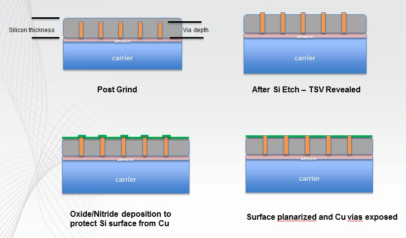
Leti gave an update on the 3DICE program being done under the European Unions 7th Framework with partners Datacon, Disco, EVG and ST Micro. Below find the unit operations that are part of the program and those responsible. They have concluded that B2F has less operations and is easier to accomplish than F2F.

Back to face attach can be done with die attach film, full sheet bonding layer or patterned bonding layer.

B2F pick and place with a Datacon 2200 can reportedly handle 20um thick die with 7um accuracy in 3 sec. Plasma stress relief allows for thin die handling by increasing die strength.

Thin die encapsulation can be accomplished in several ways i.e by conformal CVD deposition (oxide or parylene), by spin/spray coating of solutions (BCB, PI, ALX) or by film lamination. Die are bevel cut at 45 degrees to make subsequent metallization easier.

Thermo-mechanical stress in these combinations were examined.


EVG gave more details on the release process for their ZoneBond TB/DB (temp bond/debond) process.


- Adhesive ring dissolution is enhanced by magasonics                                                                                   
- Low force, room temperature separation                                                                                                        
- Compatible with both glass and Si carriers                                                                                                       
- Adhesives are (solvent)cleanable                                                                                                                    
- Platform enables use of a wide range of materials, i.e. ZoneBond Open Platform

The anti sticking layer showed a temperature stability up to 300C for 20 min. Carrier wafers were bonded and debonded 25x.

Rolf Aschenbrenner of the Fraunhoffer IZM made an in depth presentation on "Molding
technologies  - A new way for system integration" specifically looking at options for today's transfer molding and compression molding technologies.


While transfer molding has been used for years to make plastic packaged parts, compression molding has recently become in vogue as part of the embedded chip technology package, i.e molded reconfigured wafers.


They propose the following roadmap for system integration with molding.


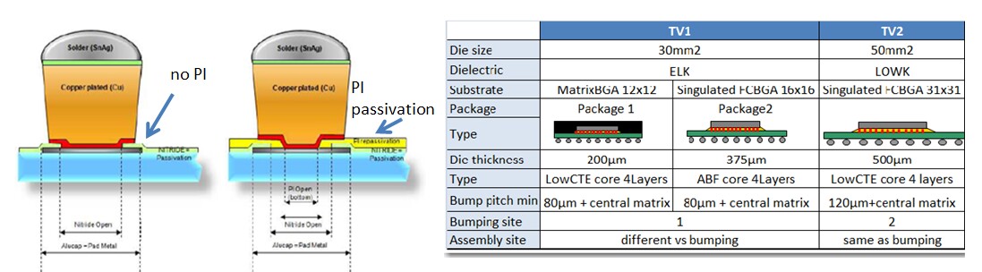
ST Micro presented some electromigration details on SnAgCu interconnect for WLB packages.
They find that:
- IMC induces resistance increase right after stress beginning
- Electrical open is due to voiding in solder, at Cu3Sn interface, after Cu6Sn5 disappeared
Since the electrical opens are due to voids at the RDL/solder interface a solution is to insure that the enclosure around the solder ball is large enough and increase the RDL thickness as much as possible.  


We will have more MINAPAD review in next week's IFTLE.

For all the latest in 3DIC and Advanced Packaging stay linked to IFTLE..........................

10 Must-Read Insights from the Leading Edge:
1. Apple and TSVs, top chip makers, and "betting the ranch"


This post investigated Apple's possible move to TSVs for its A6 chip, and compared capex numbers to the Western trope of "betting the ranch." Apple's semiconductor roadmap, and the advanced packaging technology of TSVs combined for a compelling read. Link: http://www.electroiq.com/blogs/insights_from_leading_edge/2012/02/iftle-88-apple-tsv-interposer-rumors-betting-the-ranch-tsv-for-sony-ps-4-top-chip-fabricators-i.html

2. LED market is about to explode

While Insights from the Leading Edge covers a great deal of 3D packaging news, that doesn't mean that there are no other very significant packaging evolutions and market opportunities going on at the same time. Certainly the LED space is one of those, Dr. Garrou said, and readers agreed.

Link: http://www.electroiq.com/blogs/insights_from_leading_edge/2011/11/iftle-75-led-market-is-about-to-explode.html

3. Bidding Adieu to Lester Lightbulb

Lester Lightbulb has become something of a favorite character on Insights from the Leading Edge, as Dr. Garrou carries out an in-home energy/cost savings analysis of conventional incandescent lightbulbs, CFLs, and LEDs.

Link: http://www.electroiq.com/blogs/insights_from_leading_edge/2011/08/iftle-63-bidding-adieu-to-lester-lightbulb.html

4. Advances in CMOS Image Sensing

In the fall of 2007, Toshiba first announced the commercialization of TSV in a CMOS image sensor (CIS). The next step of circuit repartitioning and stacking was interrupted by back side imaging, which flipped the chip over and let the light enter through the least obstructed side to let more light in per pixel. Now, we consider today's CIS advances.

Link: http://www.electroiq.com/blogs/insights_from_leading_edge/2012/02/iftle-89-advances-in-cmos-image-sensing.html

5. Cell Phones and Memory Consolidation

The cellphone continues to pull in the functionality of digital cameras, PDAs, GPS navigators, mobile TV and numerous other applications. It is quickly becoming the dominant market driver for virtually all of these functions.

Link: http://www.electroiq.com/blogs/insights_from_leading_edge/2011/10/iftle-69-cell-phones-and-memory-consolidation.html


6. How Xilinx fit 6.8B transistors on its 2.5D FPGA

Garrou reviews Xilinx's new FPGA, with 10,000 connections on a silicon interposer, using "2.5D packaging."

Link: http://www.electroiq.com/blogs/insights_from_leading_edge/2011/10/iftle-73-xilinx-shows-2-5d-virtex-7-at-imaps-2011.html

7. MEPTEC 2.5, 3D and beyond

Reporting from MEPTEC and SEMI's "2.5D, 3D and Beyond Bringing 3D Integration to the Packaging Mainstream" Conference in 2011, Dr. Garrou shares highlights from Amkor, GLOBALFOUNDRIES, and other presenters.

Link: http://www.electroiq.com/blogs/insights_from_leading_edge/2011/11/iftle-77-meptec-2-5-3d-and-beyond.html

8. Fine Pitch Microjoints, Cu Pillar Bump-on-Lead, Xilinx Interposer Reliability

Dr. Garrou looks at packaging activities at the 2011 ECTC, including presentations from Qualcomm and STATS ChipPAC, Fraunhofer IZM, Xilinx (interposers!), and others.

Link: http://www.electroiq.com/blogs/insights_from_leading_edge/2011/07/iftle-58-fine-pitch-microjoints-cu-pillar-bump-on-lead-xilinx-interposer-reliability.html

9. TSV from 1999 to today, and more on the Micron HMC

Dr. Garrou shows us the evolution of TSV from 1999 through to today, checks in on MU's HMC, and analyzes some recent packaging news.

Link: http://www.electroiq.com/blogs/insights_from_leading_edge/2012/04/iftle-95-3dic-time-flies-when-you-re-having-fun-further-details-on-the-micron-hmc-equipment-su.html

10. Defining 3D, and Canon's packaging equipment foray

Garrou explains the variety of 3D packaging terms with a little help from "Raymond J. Johnson Jr." He also notes Canon's back-end equipment entry.

Link: http://www.electroiq.com/blogs/insights_from_leading_edge/2011/08/iftle-62-3d-and-interposers-nomenclature-confusion-equipment-market-shift-to-pkging-continues.html

Here's to 100 more Insights from the Leading Edge blog posts!